


TABLE OF CONTENTS
viii EPSON S1C33L03 TECHNICAL MANUAL
VI SDRAM CONTROLLER BLOCK
VI-1 INTRODUCTION......................................................................................................... B-VI-1-1
VI-2 SDRAM INTERFACE ................................................................................................. B-VI-2-1
Outline of SDRAM Interface......................................................................................................B-VI-2-1
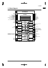
SDRAM Controller Block Diagram............................................................................................B-VI-2-1
I/O Pins and Connection ...........................................................................................................B-VI-2-2
I/O Pins...........................................................................................................................B-VI-2-2
Connection Examples....................................................................................................B-VI-2-2
SDRAM Controller Configuration..............................................................................................B-VI-2-5
Setting PLL.....................................................................................................................B-VI-2-5
BCU Configuration.........................................................................................................B-VI-2-5
SDRAM Setting Conditions ...........................................................................................B-VI-2-6
SDRAM Operation...................................................................................................................B-VI-2-12
Synchronous Clock......................................................................................................B-VI-2-12
Power-up and Initialization ..........................................................................................B-VI-2-13
SDRAM Commands ....................................................................................................B-VI-2-14
Burst Read Cycle.........................................................................................................B-VI-2-15
Single Read/Single Write.............................................................................................B-VI-2-16
Refresh Mode ..............................................................................................................B-VI-2-17
Power-down Mode.......................................................................................................B-VI-2-19
Bus Release Procedure...............................................................................................B-VI-2-19
I/O Memory of SDRAM Interface ............................................................................................B-VI-2-21
Programming Notes.................................................................................................................B-VI-2-32
Examples of SDRAM Controller Initialization Program ..........................................................B-VI-2-33
VII LCD CONTROLLER BLOCK
VII-1 INTRODUCTION........................................................................................................ B-VII-1-1
VII-2 LCD CONTROLLER.................................................................................................. B-VII-2-1
Overview...................................................................................................................................B-VII-2-1
Features........................................................................................................................B-VII-2-1
Block Diagram...............................................................................................................B-VII-2-3
I/O Pins of the LCD Controller..................................................................................................B-VII-2-4
System Settings........................................................................................................................B-VII-2-5
Setting the BCU ............................................................................................................B-VII-2-5
Display Memory ............................................................................................................B-VII-2-5
LCD Controller Setting Procedure................................................................................B-VII-2-6
Clock .............................................................................................................................B-VII-2-7
Setting the LCD Panel..............................................................................................................B-VII-2-8
Types of Panels ............................................................................................................B-VII-2-8
Resolution .....................................................................................................................B-VII-2-8
Display Modes ..............................................................................................................B-VII-2-9
Look-up Tables .......................................................................................................... B-VII-2-11
Frame Rates .............................................................................................................. B-VII-2-19
Other Settings............................................................................................................ B-VII-2-20
Display Control ...................................................................................................................... B-VII-2-21
Controlling LCD Power Up/Down.............................................................................. B-VII-2-21
Reading/Writing Display Data ................................................................................... B-VII-2-22
Setting the Display Start Address ............................................................................. B-VII-2-22
Split-Screen Display .................................................................................................. B-VII-2-23