VI SDRAM CONTROLLER BLOCK: SDRAM INTERFACE
B-VI-2-28 EPSON S1C33L03 FUNCTION PART
SDRIS: Initial command sequence (D4) / SDRAM control register (0x39FFC1)
Select the SDRAM initialization sequence.
Write "1": 1. Precharge → 2. Mode Register Set → 3. Refresh
Write "0": 1. Precharge → 2. Refresh → 3. Mode Register Set
Read: Valid
In accordance with the specifications of the SDRAM, select a sequence to determine the order the commands are
sent to initialize the SDRAM. Initialization of the SDRAM is initiated by writing "1" to SDRINI (D6/0x39FFC1).
At cold start, SDRIS is set to "0" (1. Precharge → 2. Refresh → 3. Mode Register Set). At hot start, SDRIS retains
its status before being initialized.
SDRCLK: Keep SDRAM clock during self-refresh (D3) / SDRAM control register (0x39FFC1)
Select whether or not to stop the SDRAM clock during self-refresh.
Write "1": Kept outputting
Write "0": Stopped
Read: Valid
Writing "0" to SDRCLK causes the SDRAM clock output from the BCLK pin to stop and to remain off while the
SDRAM is self-refreshed. This helps to reduce the chip's current consumption. Note that when the bus is released,
the BCLK pin goes into a high-impedance state.
If SDRCLK = "1", the SDRAM clock is always output from the BCLK pin even while the SDRAM is self-
refreshed or the bus is released.
At cold start, SDRCLK is set to "1" (kept outputting). At hot start, SDRCLK retains its status before being
initialized.
SDRCA1–SDRCA0: SDRAM page size (D[6:5]) / SDRAM address configuration register (0x39FFC2)
Set the SDRAM page size (column addressing range).
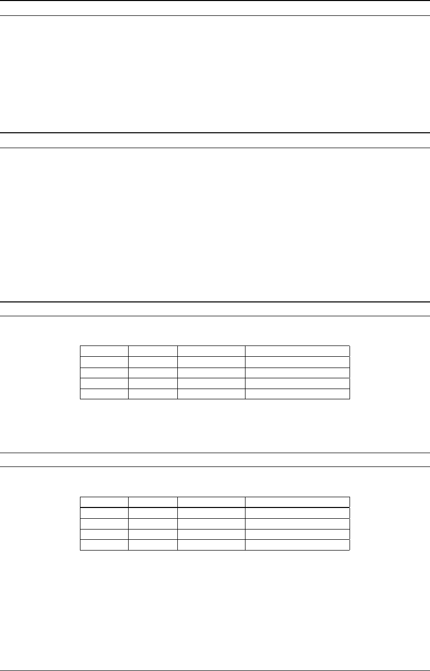
Table 2.15 Setting Column Addressing Range (Page Size)
SDRCA1 SDRCA0 Column size Column address (pin) used
00 256SDA0–SDA7 (default)
01 512 SDA0–SDA8
10 1,024 SDA0–SDA9
11 – –
The contents set here are applied to all of areas 7, 8, 13, and 14 that are set for SDRAM.
SDRCA can be read to obtain its set value.
At cold start, SDRCA is set to "0" (256). At hot start, SDRCA retain its status before being initialized.
SDRRA1–SDRRA0:
SDRAM row addressing range (D[3:2]) / SDRAM address configuration register (0x39FFC2)
Set the SDRAM row addressing range.
Table 2.16 Setting Row Addressing Range
SDRRA1 SDRRA0 Row size Row address (pin) used
00 2KSDA0–SDA10 (default)
01 4K SDA0–SDA11
10 8K SDA0–SDA12
11 – –
The contents set here are applied to all of areas 7, 8, 13, and 14 that are set for SDRAM.
SDRRA can be read to obtain its set value.
At cold start, SDRRA is set to "0" (2K). At hot start, SDRRA retain its status before being initialized.


