


III PERIPHERAL BLOCK: INPUT/OUTPUT PORTS
B-III-9-6 EPSON S1C33L03 FUNCTION PART
I/O Memory of I/O Ports
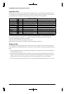
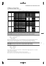
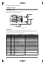
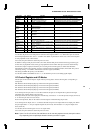
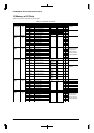
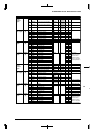
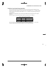
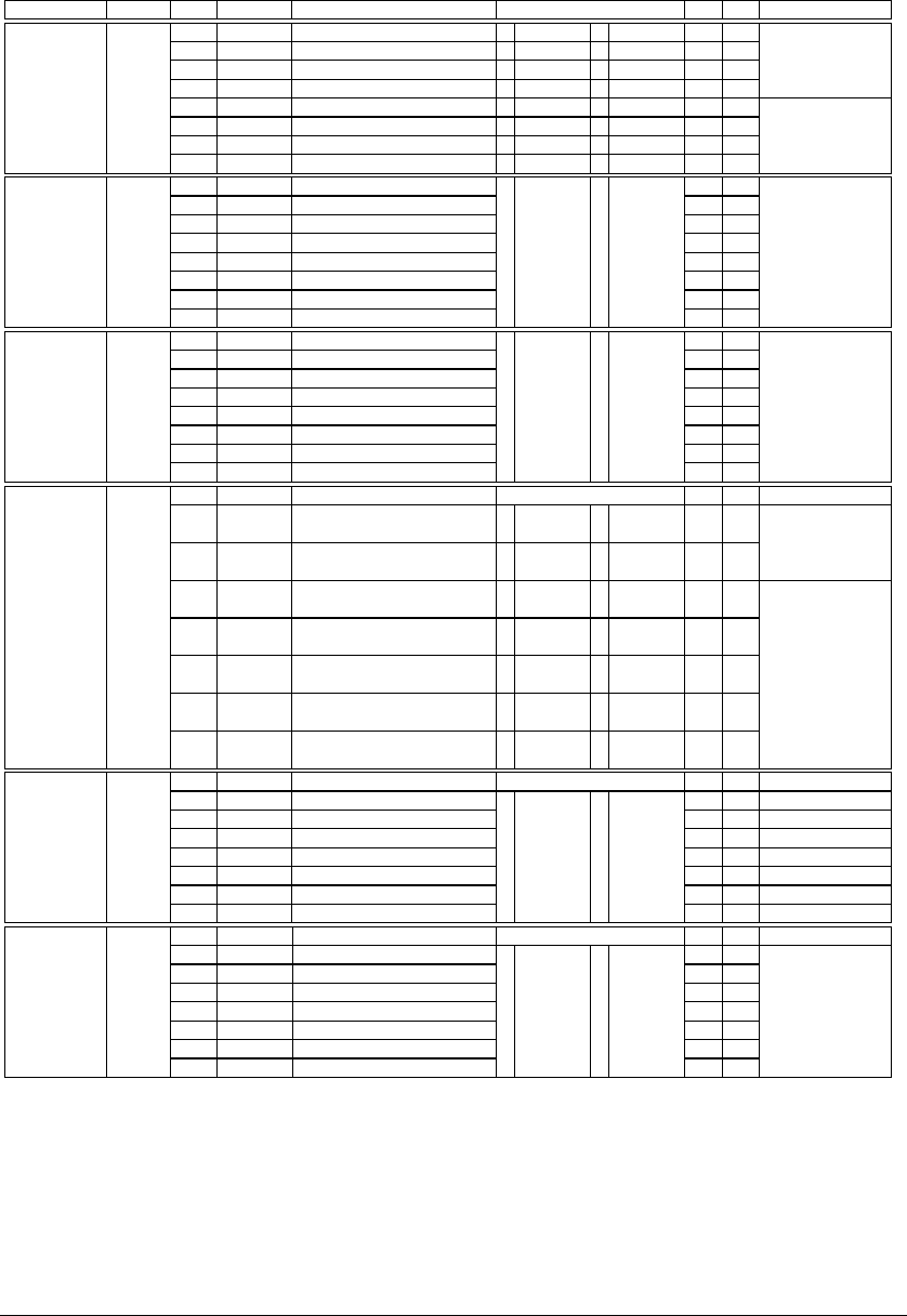
Table 9.4 shows the control bits of the I/O ports.
Table 9.4 Control Bits of I/O Ports
NameAddressRegister name Bit Function Setting Init. R/W Remarks
CFP07
CFP06
CFP05
CFP04
CFP03
CFP02
CFP01
CFP00
D7
D6
D5
D4
D3
D2
D1
D0
P07 function selection
P06 function selection
P05 function selection
P04 function selection
P03 function selection
P02 function selection
P01 function selection
P00 function selection
0
0
0
0
0
0
0
0
R/W
R/W
R/W
R/W
R/W
R/W
R/W
R/W
Extended functions
(0x402DF)
00402D0
(B)
1 #SRDY1 0 P07
1 #SCLK1 0 P06
1 SOUT1 0 P05
1 SIN1 0 P04
1 #SRDY0 0 P03
1 #SCLK0 0 P02
1 SOUT0 0 P01
1 SIN0 0 P00
P0 function
select register
P07D
P06D
P05D
P04D
P03D
P02D
P01D
P00D
D7
D6
D5
D4
D3
D2
D1
D0
P07 I/O port data
P06 I/O port data
P05 I/O port data
P04 I/O port data
P03 I/O port data
P02 I/O port data
P01 I/O port data
P00 I/O port data
0
0
0
0
0
0
0
0
R/W
R/W
R/W
R/W
R/W
R/W
R/W
R/W
00402D1
(B)
1 High 0 LowP0 I/O port data
register
IOC07
IOC06
IOC05
IOC04
IOC03
IOC02
IOC01
IOC00
D7
D6
D5
D4
D3
D2
D1
D0
P07 I/O control
P06 I/O control
P05 I/O control
P04 I/O control
P03 I/O control
P02 I/O control
P01 I/O control
P00 I/O control
0
0
0
0
0
0
0
0
R/W
R/W
R/W
R/W
R/W
R/W
R/W
R/W
This register
indicates the values
of the I/O control
signals of the ports
when it is read. (See
detailed explanation.)
00402D2
(B)
1 Output 0 InputP0 I/O control
register
–
CFP16
CFP15
CFP14
CFP13
CFP12
CFP11
CFP10
D7
D6
D5
D4
D3
D2
D1
D0
reserved
P16 function selection
P15 function selection
P14 function selection
P13 function selection
P12 function selection
P11 function selection
P10 function selection
–
0
0
0
0
0
0
0
–
R/W
R/W
R/W
R/W
R/W
R/W
R/W
0 when being read.
Extended functions
(0x402DF)
00402D4
(B)
1 EXCL5
#DMAEND1
0 P16
1 EXCL4
#DMAEND0
0 P15
1 EXCL3
T8UF3
0 P13
1 EXCL2
T8UF2
0 P12
1 EXCL1
T8UF1
0 P11
1 EXCL0
T8UF0
0 P10
–P1 function
select register
1 FOSC1 0 P14
–
P16D
P15D
P14D
P13D
P12D
P11D
P10D
D7
D6
D5
D4
D3
D2
D1
D0
reserved
P16 I/O port data
P15 I/O port data
P14 I/O port data
P13 I/O port data
P12 I/O port data
P11 I/O port data
P10 I/O port data
–
0
0
0
0
0
0
0
–
R/W
R/W
R/W
R/W
R/W
R/W
R/W
0 when being read.00402D5
(B)
1 High 0 Low
–
P1 I/O port data
register
–
IOC16
IOC15
IOC14
IOC13
IOC12
IOC11
IOC10
D7
D6
D5
D4
D3
D2
D1
D0
reserved
P16 I/O control
P15 I/O control
P14 I/O control
P13 I/O control
P12 I/O control
P11 I/O control
P10 I/O control
–
0
0
0
0
0
0
0
–
R/W
R/W
R/W
R/W
R/W
R/W
R/W
0 when being read.
This register
indicates the values
of the I/O control
signals of the ports
when it is read. (See
detailed explanation.)
00402D6
(B)
1 Output 0 Input
–P1 I/O control
register