


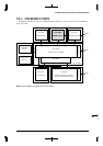


VI SDRAM CONTROLLER BLOCK: SDRAM INTERFACE
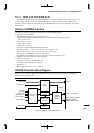
B-VI-2-6 EPSON S1C33L03 FUNCTION PART
B. When using areas 13/14 (CEFUNC = "01")
B-1. A14IO (DD)/Access control register (0x48132) = "1"
This sets areas 13/14 for internal access.
B-2. A14WT[2:0] (D[2:0])/Areas 14–13 set-up register (0x48122) = "000"
This sets areas 13/14 for no-wait access.
B-3. A14SZ (D6)/Areas 14–13 set-up register (0x48122) = SDRSZ (D6)/SDRAM advanced control register
(0x39FFC9)
Use these registers to ensure that the device size of areas 13/14 and that of the SDRAM controller are the
same, and are matched to the SDRAM data width. Both bits select 16 bits when "0" or 8 bits when "1".
B-4. A14DF[1:0] (D[5:4])/Areas 14–13 set-up register (0x48122)
If the system has an external memory device other than an SDRAM connected to it and accesses that memory
device and SDRAM in succession, set the output disable delay time of areas 13/14 to 2.5 cycles (A14DF[1:0]
= "10").
When only the SDRAM is read and no other external device is accessed, set the output disable delay time of
areas 13/14 to 0.5 cycles (A14DF[1:0] = "00") in order to reduce the SDRAM access time.
This completes the BCU settings necessary to access the SDRAM.
Make sure the BCU parameters other than those discussed above are set appropriately for the system.
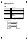
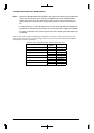
SDRAM Setting Conditions
The SDRAM interface allows the following conditions to be selected. Although SDRAM can be used in areas 7
and 8 or areas 13 and 14, these conditions are applied to all four areas and cannot be set individually for each area.
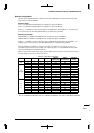
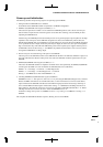
Table 2.4 SDRAM Interface Parameters
Parameter Selectable condition Initial setting Control bits
Area 7/13 configuration SDRAM or Another Another device SDRAR0(D7)/SDRAM area configuration register(0x39FFC0)
Area 8/14 configuration SDRAM or Another Another device SDRAR1(D6)/SDRAM area configuration register(0x39FFC0)
#CE7/13 pin configuration #SDCE0 or #CE7/13 #CE7/13 SDRPC0(D3)/SDRAM area configuration register(0x39FFC0)
#CE8/14 pin configuration #SDCE1 or #CE8/14 #CE8/14 SDRPC1(D2)/SDRAM area configuration register(0x39FFC0)
Page size 256, 512 or 1K 256 SDRCA[1:0](D[6:5])
/SDRAM address configuration register(0x39FFC2)
Row addressing range 2K, 4K or 8K 2K SDRRA[1:0](D[3:2])
/SDRAM address configuration register(0x39FFC2)
Number of banks 4 or 2 2 SDRBA(D1)
/SDRAM address configuration register(0x39FFC2)
Initial command sequence 1. Precharge
2. Refresh
3. Mode register
or
1. Precharge
2. Mode register
3. Refresh
1. Precharge
2. Refresh
3. Mode register
SDRIS(D4)/SDRAM control register(0x39FFC1)
Burst length 1, 2, 4 or 8 8 SDRBL[1:0](D[3:2])/SDRAM mode set-up register(0x39FFC3)
CAS latency 2 – * SDRCL[1:0](D[6:5])/SDRAM mode set-up register(0x39FFC3)
tRAS 1 to 8 clocks 8 clocks SDRTRAS[2:0](D[7:5])/SDRAM timing set-up register 1
(0x39FFC4)
tRP 1 to 4 clocks 4 clocks SDRTRP[1:0](D[4:3])/SDRAM timing set-up register 1
(0x39FFC4)
tRC 1 to 8 clocks 8 clocks SDRTRC[2:0](D[2:0])/SDRAM timing set-up register 1
(0x39FFC4)
tRCD 1 to 4 clocks 4 clocks SDRTRCD[1:0](D[7:6])/SDRAM timing set-up register 2
(0x39FFC5)
tRSC 1 or 2 clocks 2 clocks SDRTRSC(D5)/SDRAM timing set-up register 2 (0x39FFC5)
tRRD 1 to 4 clocks 4 clocks SDRTRRD[1:0](D[4:3])/SDRAM timing set-up register 2
(0x39FFC5)
∗ Always set CAS latency to 2.