


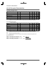
7 PRECAUTIONS ON MOUNTING
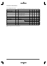
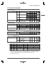
A-70 EPSON S1C33205 PRODUCT PART
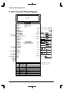
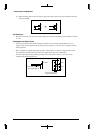
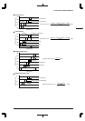
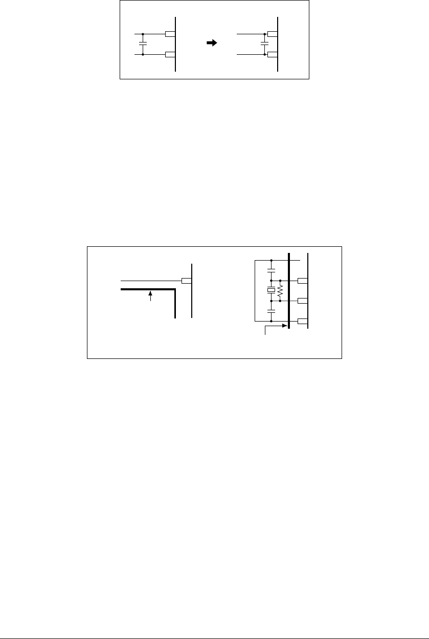
(2) When connecting between the VDD and VSS pins with a bypass capacitor, the pins should be connected
as short as possible.
V
DD
V
SS
Bypass capacitor connection example
V
DD
V
SS
A/D Converter
•When the A/D converter is not used, the power supply pin AVDDE for the analog system should be connected
to V
DDE.
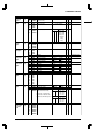
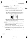
Arrangement of Signal Lines
•In order to prevent generation of electromagnetic induction noise caused by mutual inductance, do not
arrange a large current signal line near the circuits that are sensitive to noise such as the oscillation unit and
analog input unit.
•When a signal line is parallel with a high-speed line in long distance or intersects a high-speed line, noise
may generated by mutual interference between the signals and it may cause a malfunction.
Do not arrange a high-speed signal line especially near circuits that are sensitive to noise such as the
oscillation unit and analog input unit.
K60 (AD0)
Large current signal line
High-speed signal line
OSC4
OSC3
V
SS
Large current signal line
High-speed signal line
Prohibited pattern