II CORE BLOCK: BCU (Bus Control Unit)
S1C33L03 FUNCTION PART EPSON B-II-4-43
A-1
B-II
BCU
SWAITE: #WAIT enable (D0) / Bus control register (0x4812E)
Enable or disable wait cycle control via the #WAIT pin.
Write "1": Enabled
Write "0": Disabled
Read: Valid
A wait request from an SRAM device is made acceptable by writing "1" to SWAITE. The wait request signal input
from the #WAIT pin is sampled at each falling edge of the bus clock when executing an SRAM read/write cycle.
Wait cycles are inserted until the wait request signal is sampled and detected as high (inactive).
Wait control for 0 to 7 cycles can be accomplished by AxxWT without using the #WAIT pin. However, since the
setting via AxxWT is applied to every two areas, the number of wait cycles may be controlled individually in each
area or more than 7 wait cycles may be set. In such a case, use an external wait request via the #WAIT pin.
Wait requests from the #WAIT pin are ignored when SWAITE = "0".
The contents set here are applied to all areas that are set for SRAM, and are also effective for write cycles in the
areas that are set for burst ROM.
At cold start, SWAITE is set to "0" (disabled). At hot start, SWAITE retains its status before being initialized.
A3EEN: Area 3 emulation (DB) / DRAM timing set-up register (0x48130)
Select area 3 emulation mode.
Write "1": Internal ROM mode
Write "0": Emulation mode
Read: Valid
When "0" is written to A3EEN, internal ROM emulation mode is selected and the external device will be accessed
with the same condition as the internal ROM. When "1" is written, the internal ROM will be used for accessing
area 3. This bit functions the same as the EA3MD pin. The bit status and the pin status are logically ORed.
At cold start, A3EEN is set to "1" (internal ROM mode). At hot start, A3EEN retains its status before being
initialized.
CEFUNC1–CEFUNC0: #CE pin function selection (D[A:9]) / DRAM timing set-up register (0x48130)
Change the #CE pin-assigned area.
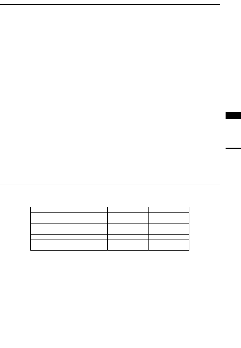
Table 4.28 #CE Output Assignment
PinCEFUNC = "00" CEFUNC = "01" CEFUNC = "1x"
#CE4 #CE4 #CE11 #CE11+#CE12
#CE5 #CE5 #CE15 #CE15+#CE16
#CE6 #CE6 #CE6 #CE7+#CE8
#CE7/#RAS0 #CE7/#RAS0 #CE13/#RAS2 #CE13/#RAS2
#CE8/#RAS1 #CE8/#RAS1 #CE14/#RAS3 #CE14/#RAS3
#CE9 #CE9 #CE17 #CE17+#CE18
#CE10EX #CE10EX #CE10EX #CE9+#CE10EX
(Default: CEFUNC = "00")
The high-order areas that are made available for use by writing "01" to CEFUNC can be larger in size than the
default low-order areas. For example, when using DRAM in default settings, the available space is 4 MB in areas 7
and 8. However, if areas 13 and 14 are used, up to 32 MB of DRAM can be used. The same applies to the other
areas.
Furthermore, when CEFUNC is set to "10" or "11", four chip enable signal is expanded into two area size.
At cold start, CEFUNC is set to "00". At hot start, CEFUNC retains its status before being initialized.


