


VII LCD CONTROLLER BLOCK: LCD CONTROLLER
B-VII-2-4 EPSON S1C33L03 FUNCTION PART
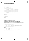
I/O Pins of the LCD Controller
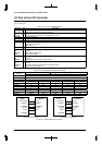
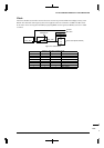
Table 2.1 lists the input/output pins of the LCD controller. Table 2.2 shows the pin configurations classified by
type of LCD panel.
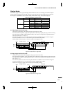
Table 2.1 I/O Pins of the LCD Controller
Pin name I/O Description
FPDAT[7:4] O 4-bit LCD-panel data bus
8-bit LCD-panel data bus, four high-order bits
FPDAT[3:0]
GPO[6:3]
O8-bit LCD-panel data bus, four low-order bits
General-purpose output when a 4-bit LCD panel is used
FPFRAME O Frame-pulse output
FPLINE O Line-pulse output
FPSHIFT O Shift-clock output
DRDY O LCD backplane bias (MOD)
Shift clock 2 (FPSHIFT2)
See Table 2.2.
LCDPWR O LCD power-supply control output (active high)
GPIO0
P34
#BUSREQ
#CE6
I/O GPIO0 See "Control of GPIO pins".
I/O port
Bus-release-request input
Area-6 chip enable
GPIO1
P35
#BUSACK
I/O GPIO1 See "Control of GPIO pins".
I/O port
Acknowledge output for bus release request
GPIO2
P31
#BUSGET
#GARD
I/O GPIO2 See "Control of GPIO pins".
I/O port
Bus-status-monitor signal output for bus release request
GA-area read signal output
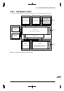
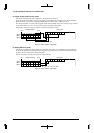
Table 2.2 Pin Configurations by Type of LCD Panel
Monochrome passive panel Color passive panel
Pin name
4 bits 8 bits 4 bits 8-bit format 1 8-bit format 2
FPFRAME FPFRAME
FPLINE FPLINE
DRDY MOD MOD MOD FPSHIFT2 MOD
FPDAT7 D3 D7 D3 D7 D7
FPDAT6 D2 D6 D2 D6 D6
FPDAT5 D1 D5 D1 D5 D5
FPDAT4 D0 D4 D0 D4 D4
FPDAT3 GPO6 D3 GPO6 D3 D3
FPDAT2 GPO5 D2 GPO5 D2 D2
FPDAT1 GPO4 D1 GPO4 D1 D1
FPDAT0 GPO3 D0 GPO3 D0 D0
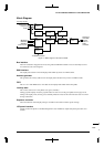
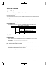
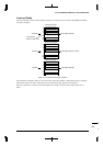
FPDAT[7:0]
FPSHIFT
FPFRAME
FPLINE
DRDY
LCDPWR
S1C33
D[7:0]
FPSHIFT
FPFRAME
FPLINE
MOD
LCD panel
FPDAT[3:0]
FPSHIFT
FPFRAME
FPLINE
DRDY
LCDPWR
S1C33
D[3:0]
FPSHIFT
FPFRAME
FPLINE
MOD
LCD panel
8-bit passive LCD panel 4-bit passive LCD panel
Figure 2.2 Typical LCD-Panel Connections