III PERIPHERAL BLOCK: INPUT/OUTPUT PORTS
S1C33L03 FUNCTION PART EPSON B-III-9-15
A-1
B-III
I/O
Selecting input pins
For the FPK1 interrupt system, a four-bit input pin group can be selected from the four predefined groups.
For the FPK0 system, a five-bit input pin group can be selected.
Table 9.7 shows the control bits and the selectable groups for each factor.
Table 9.7 Selecting Pins for Key Input Interrupts
Interrupt SPPK settings
factor
Control bit
11 10 01 00
FPK1 SPPK1[1:0] (D[3:2])/Key input interrupt select register (0x402CA) P2[7:4] P0[7:4] K6[7:4] K6[3:0]
FPK0 SPPK0[1:0] (D[1:0])/Key input interrupt select register (0x402CA) P2[4:0] P0[4:0] K6[4:0] K5[4:0]
Conditions for key input-interrupt generation
The key input interrupt circuit has two input mask registers (SMPK0[4:0] for FPK0 and SMPK1[3:0] for
FPK1) and two input comparison registers (SCPK0[4:0] for FPK0 and SCPK0[3:0] for FPK1) to set input-
interrupt conditions.
The input mask register SMPK is used to mask the input pin that is not used for an interrupt. This register
masks each input pin, whereas the interrupt enable register of the interrupt controller masks the interrupt
factor for each interrupt group.
The input comparison register SCPK is used to select whether an interrupt for each input port is to be
generated at the rising or falling edge of the input.
A change in state occurs so that the input pin enabled for interrupt by the interrupt mask register SMPK and
the content of the input comparison register SCPK become unmatched after being matched, the interrupt
factor flag FK is set to "1" and, if other interrupt conditions are met, an interrupt is generated.
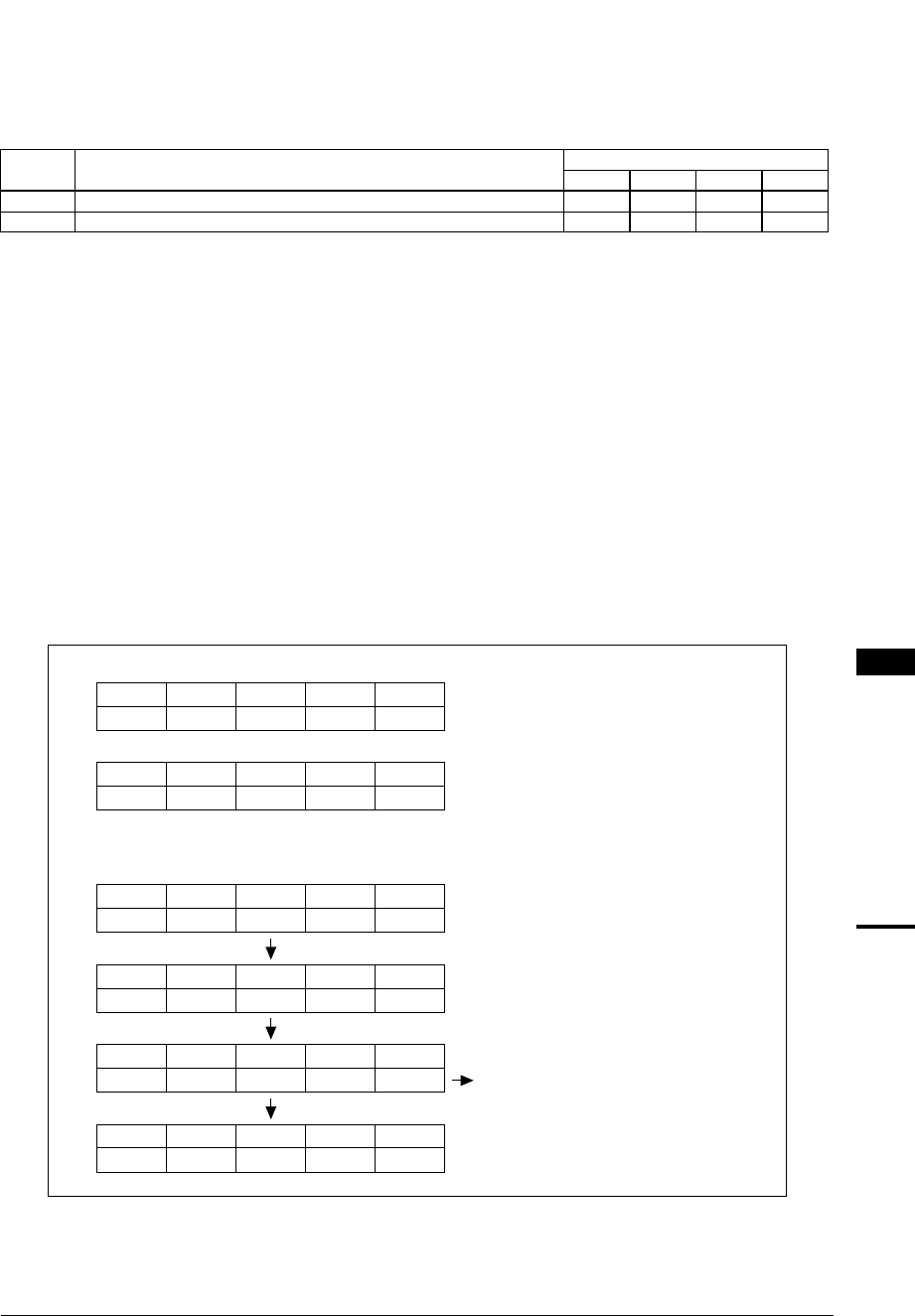
Figure 9.5 shows cases in which a FPK0 interrupt is generated. Here, it is assumed that the K5[4:0] pins are
selected for the input-pin group and the control register of the interrupt controller is set so as to enable
generation of a FPK0 interrupt.
Intput mask register SMPK0
Input comparison register SCPK0
SMPK04
1
SMPK03
1
SMPK02
1
SMPK01
1
SMPK00
0
Input port K5
(1)
(Initial value)
Interrupt generation
K54
1
SCPK04
1
SCPK03
1
SCPK02
0
SCPK01
1
SCPK00
0
With the settings shown above, FPK0 interrupt is generated under the condition shown below.
(2)
K54
1
(3)
K54
1
(4)
K54
1
K53
1
K52
0
K51
1
K50
0
K53
1
K52
0
K51
1
K50
1
K53
0
K52
0
K51
1
K50
0
K53
0
K52
1
K51
1
K50
0
Because interrupt has been disabled for
K50, interrupt will be generated when non-
conformity occurs between the contents of
the four bits K51–K54 and the four bits
input comparison register SCPK0[4:1].
Figure 9.5 FPK0 Interrupt Generation Example (when K5[4:0] is selected by SPPK[1:0])


