


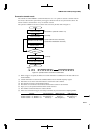
V DMA BLOCK: IDMA (Intelligent DMA)
S1C33L03 FUNCTION PART EPSON B-V-3-5
A-1
B-V
IDMA
IDMA Invocation
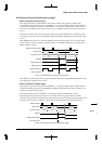
The triggers by which IDMA is invoked have the following three causes:
1. Interrupt factor in an internal peripheral circuit
2. Trigger in the software application
3. Link setting
Enabling/disabling DMA transfer
The IDMA controller is enabled by writing "1" to the IDMA enable bit IDMAEN (D0) / IDMA enable
register (0x48205), and is ready to accept the triggers described above. However, before enabling a DMA
transfer, be sure to set the base address and the control information for the channel to be invoked correctly. If
IDMAEN is set to "0", no IDMA invocation request is accepted.
IDMA invocation by an interrupt factor in internal peripheral circuits
Some internal peripheral circuits that have an interrupt generating function can invoke IDMA by an interrupt
factor in that circuit. The IDMA channel numbers corresponding to such IDMA invocation are predetermined.
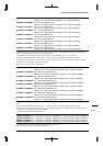
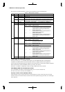
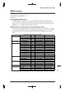
The relationship between the interrupt factors that have this function and the IDMA channels is shown in
Table 3.2.
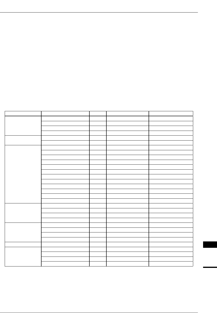
Table 3.2 Interrupt Factors Used to Invoke IDMA
Peripheral circuit Interrupt factor IDMA Ch. IDMA request bit IDMA enable bit
Ports Port input 0 1 RP0 (D0/0x40290) DEP0 (D0/0x40294)
Port input 1 2 RP1 (D1/0x40290) DEP1 (D1/0x40294)
Port input 2 3 RP2 (D2/0x40290) DEP2 (D2/0x40294)
Port input 3 4 RP3 (D3/0x40290) DEP3 (D3/0x40294)
High-speed DMA Ch.0, end of transfer 5 RHDM0 (D4/0x40290) DEHDM0 (D4/0x40294)
Ch.1, end of transfer 6 RHDM1 (D5/0x40290) DEHDM1 (D5/0x40294)
16-bit programmable Timer 0 comparison B 7 R16TU0 (D6/0x40290) DE16TU0 (D6/0x40294)
timer Timer 0 comparison A 8 R16TC0 (D7/0x40290) DE16TC0 (D7/0x40294)
Timer 1 comparison B 9 R16TU1 (D0/0x40291) DE16TU1 (D0/0x40295)
Timer 1 comparison A 10 R16TC1 (D1/0x40291) DE16TC1 (D1/0x40295)
Timer 2 comparison B 11 R16TU2 (D2/0x40291) DE16TU2 (D2/0x40295)
Timer 2 comparison A 12 R16TC2 (D3/0x40291) DE16TC2 (D3/0x40295)
Timer 3 comparison B 13 R16TU3 (D4/0x40291) DE16TU3 (D4/0x40295)
Timer 3 comparison A 14 R16TC3 (D5/0x40291) DE16TC3 (D5/0x40295)
Timer 4 comparison B 15 R16TU4 (D6/0x40291) DE16TU4 (D6/0x40295)
Timer 4 comparison A 16 R16TC4 (D7/0x40291) DE16TC4 (D7/0x40295)
Timer 5 comparison B 17 R16TU5 (D0/0x40292) DE16TU5 (D0/0x40296)
Timer 5 comparison A 18 R16TC5 (D1/0x40292) DE16TC5 (D1/0x40296)
8-bit programmable Timer 0 underflow 19 R8TU0 (D2/0x40292) DE8TU0 (D2/0x40296)
timer Timer 1 underflow 20 R8TU1 (D3/0x40292) DE8TU1 (D3/0x40296)
Timer 2 underflow 21 R8TU2 (D4/0x40292) DE8TU2 (D4/0x40296)
Timer 3 underflow 22 R8TU3 (D5/0x40292) DE8TU3 (D5/0x40296)
Serial interface Ch.0 receive buffer full 23 RSRX0 (D6/0x40292) DESRX0 (D6/0x40296)
Ch.0 transmit buffer empty 24 RSTX0 (D7/0x40292) DESTX0 (D7/0x40296)
Ch.1 receive buffer full 25 RSRX1 (D0/0x40293) DESRX1 (D0/0x40297)
Ch.1 transmit buffer empty 26 RSTX1 (D1/0x40293) DESTX1 (D1/0x40297)
A/D converter End of A/D conversion 27 RADE (D2/0x40293) DEADE (D2/0x40297)
Ports Port input 4 28 RP4 (D4/0x40293) DEP4 (D4/0x40297)
Port input 5 29 RP5 (D5/0x40293) DEP5 (D5/0x40297)
Port input 6 30 RP4 (D6/0x40293) DEP4 (D6/0x40297)
Port input 7 31 RP7 (D7/0x40293) DEP7 (D7/0x40297)