


I OUTLINE: LIST OF PINS
S1C33L03 FUNCTION PART EPSON B-I-3-7
A-1
B-I
Pin
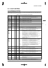
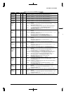
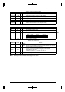
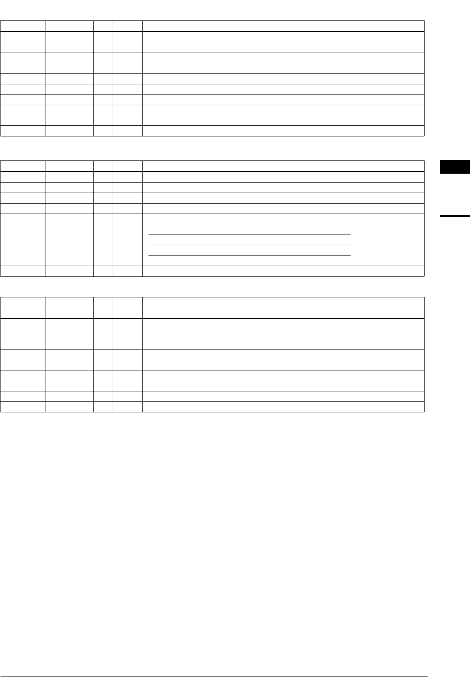
Table 3.4 List of Pins for LCD Controller
Pin name Pin No. I/O Pull-up Function
FPDAT[7:4] 13–16 O – 4 high-order bits of data bus for 8-bit LCD panels
Data bus for 4-bit LCD panels
FPDAT[3:0]
GPO[6:3]
17–20 O – FPDAT[3:0]: 4 low-order bits of data bus for 8-bit LCD panels
GPO[6:3]: General-purpose outputs when a 4-bit LCD panel is used
FPFRAME 23 O – Frame pulse output
FPLINE 24 O – Line pulse output
FPSHIFT 25 O – Shift clock output
DRDY(MOD)
(FPSHIFT2)
22 O – MOD: LCD backplane bias (for panels other than 8-bit color panel format 1)
FPSHIFT2: Second shift clock (for 8-bit color panel format 1)
LCDPWR 26 O – LCD power control output (active high)
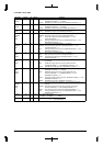
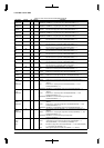
Table 3.5 List of Pins for Clock Generator
Pin name Pin No. I/O Pull-up Function
OSC1 68 I – Low-speed (OSC1) oscillation input (32 kHz crystal oscillator or external clock input)
OSC2 67 O – Low-speed (OSC1) oscillation output
OSC3 129 I – High-speed (OSC3) oscillation input (crystal/ceramic oscillator or external clock input)
OSC4 128 O – High-speed (OSC3) oscillation output
PLLS[1:0] 112,113 I – PLL set-up pins
PLLS1 PLLS0 fin (fOSC3)fout (fPSCIN)
1110–25MHz 20–50MHz
0110–12.5MHz 40–50MHz
00PLL is not used L
PLLC 115 – – Capacitor connecting pin for PLL
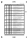
Table 3.6 List of Other Pins
Pin name Pin No. I/O
Pull-up
/down
Function
ICEMD 125 I Pull-
down
High-impedance control input pin
When this pin is set to High, all the output pins go into high-impedance state. This makes
it possible to disable the S1C33 chip on the board.
DSIO 117 I/O Pull-up Serial I/O pin for debugging
This pin is used to communicate with the debugging tool S5U1C33000H.
#X2SPD 140 I – Clock doubling mode set-up pin
1: CPU clock = bus clock × 1, 0: CPU clock = bus clock × 2
#NMI 130 I Pull-up NMI request input pin
#RESET 69 I Pull-up Initial reset input pin
Note: "#" in the pin names indicates that the signal is low active.