III PERIPHERAL BLOCK: CLOCK TIMER
S1C33L03 FUNCTION PART EPSON B-III-7-9
A-1
B-III
CTM
TCRUN: Clock timer RUN/STOP control (D0) / Clock timer Run/Stop register (0x40151)
Controls the RUN/STOP of the clock timer.
Write "1": RUN
Write "0": STOP
Read: Valid
The clock timer is made to start counting by writing "1" to the TCRUN register and made to stop by writing "0".
The timer data is retained even in the STOP state. The timer can also be made to start counting from the retained
data by changing its state from STOP to RUN.
The TCRUN register is not initialized at initial reset.
TCD7–TCD0:1–128 Hz counter data (D[7:0]) / Clock timer divider register (0x40153)
TCMD5–TCMD0:Second counter data (D[5:0]) / Clock timer second register (0x40154)
TCHD5–TCHD0:Minute counter data (D[5:0]) / Clock timer minute register (0x40155)
TCDD4–TCDD0:Hour counter data (D[4:0]) / Clock timer hour register (0x40156)
TCND15–TCND0:Day counter data (D[7:0]) / Clock timer day (high-order) register (0x40158)
(D[7:0]) / Clock timer day (low-order) register (0x40157)
Data can be read out from each counter.
The minute, hour, and day counters allow data to be written to, in addition to being read out.
The 1–128 Hz counter and seconds counter are read-only, so writing to these registers is ignored.
The unused high-order bits at each address of the second, minute, and hour counter data are always "0" when read
out.
The counter data is not initialized at initial reset.
TCCH5–TCCH0:Minute-comparison data (D[5:0]) / Clock timer minute-comparison register (0x40159)
TCCD4–TCCD0:Hour-comparison data (D[4:0]) / Clock timer hour-comparison register (0x4015A)
TCCN4–TCCN0:Day-comparison data (D[4:0]) / Clock timer day-comparison register (0x4015B)
Set a day on which and a time at which an alarm is to be generated.
The comparison data register corresponding to the alarm factor selected using the TCASE register is compared
with the counter data, and when the data matches, an alarm interrupt request is generated.
The day-comparison data is compared with the 5 low-order bits of the day counter.
Each register can be read out.
These registers are not initialized at initial reset.
TCISE2–TCISE0: Interrupt factor selection (D[7:5]) / Clock timer interrupt control register (0x40152)
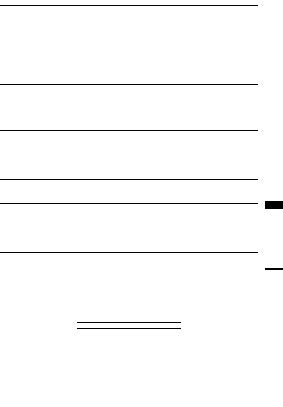
Selects the factor for which the clock timer interrupt is to be generated.
Table 7.6 Selecting Interrupt Factor
TCISE2 TCISE1 TCISE0 Interrupt factor
111None
1101 day
1011 hour
1001 minute
0111 Hz
0102 Hz
0018 Hz
00032 Hz
When the clock timer interrupt is enabled, an interrupt is generated cyclically at each falling edge of the selected
signal. If you the interrupt caused by these factors is not be used set TCISE to "111".
TCISE is not initialized at initial reset.


