


V DMA BLOCK: HSDMA (High-Speed DMA)
S1C33L03 FUNCTION PART EPSON B-V-2-33
A-1
B-V
HSDMA
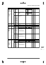
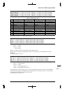
S0ADRL15–S0ADRL0:Ch. 0 source address[15:0]
(D[F:0]) / Ch. 0 low-order source address set-up register (0x48224)
S0ADRH11–S0ADRH0:Ch. 0 source address[27:16]
(D[B:0]) / Ch. 0 high-order source address set-up register (0x48226)
S1ADRL15–S1ADRL0:Ch. 1 source address[15:0]
(D[F:0]) / Ch. 1 low-order source address set-up register (0x48234)
S1ADRH11–S1ADRH0:Ch. 1 source address[27:16]
(D[B:0]) / Ch. 1 high-order source address set-up register (0x48236)
S2ADRL15–S2ADRL0:Ch. 2 source address[15:0]
(D[F:0]) / Ch. 2 low-order source address set-up register (0x48244)
S2ADRH11–S2ADRH0:Ch. 2 source address[27:16]
(D[B:0]) / Ch. 2 high-order source address set-up register (0x48246)
S3ADRL15–S3ADRL0:Ch. 3 source address[15:0]
(D[F:0]) / Ch. 3 low-order source address set-up register (0x48254)
S3ADRH11–S3ADRH0:Ch. 3 source address[27:16]
(D[B:0]) / Ch. 3 high-order source address set-up register (0x48256)
In dual-address mode, these bits are used to specify a source address. In single-address mode, an external memory
address at the destination or source of transfer is specified.
Use SxADRL to set the 16 low-order bits of the address and SxADRH to set the 12 high-order bits.
Be sure to disable DMA transfers (HSx_EN = "0") before writing or reading to and from these registers.
The address is incremented or decremented (as set by SxIN) according to the transfer data size each time a DMA
transfer in the corresponding channel is performed.
At initial reset, these bits are not initialized.
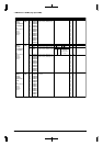
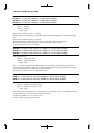
D0ADRL15–D0ADRL0:Ch. 0 destination address[15:0]
(D[F:0]) / Ch. 0 low-order destination address set-up register (0x48228)
D0ADRH11–D0ADRH0:Ch. 0 destination address[27:16]
(D[B:0]) / Ch. 0 high-order destination address set-up register (0x4822A)
D1ADRL15–D1ADRL0:Ch. 1 destination address[15:0]
(D[F:0]) / Ch. 1 low-order destination address set-up register (0x48238)
D1ADRH11–D1ADRH0:Ch. 1 destination address[27:16]
(D[B:0]) / Ch. 1 high-order destination address set-up register (0x4823A)
D2ADRL15–D2ADRL0:Ch. 2 destination address[15:0]
(D[F:0]) / Ch. 2 low-order destination address set-up register (0x48248)
D2ADRH11–D2ADRH0:Ch. 2 destination address[27:16]
(D[B:0]) / Ch. 2 high-order destination address set-up register (0x4824A)
D3ADRL15–D3ADRL0:Ch. 3 destination address[15:0]
(D[F:0]) / Ch. 3 low-order destination address set-up register (0x48258)
D3ADRH11–D3ADRH0:Ch. 3 destination address[27:16]
(D[B:0]) / Ch. 3 high-order destination address set-up register (0x4825A)
In dual-address mode, these bits are used to specify a destination address. In single-address mode, these bits are not
used.
Be sure to disable DMA transfers (HSx_EN = "0") before writing or reading to and from these registers.
The address is incremented or decremented (as set by DxIN) according to the transfer data size each time a DMA
transfer in the corresponding channel is performed.
At initial reset, these bits are not initialized.
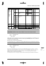
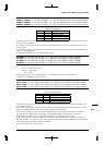
PHSD0L2–PHSD0L0: Ch. 0 interrupt level (D[2:0]) / HSDMA Ch. 0/1 interrupt priority register (0x40263)
PHSD1L2–PHSD1L0: Ch. 1 interrupt level (D[6:4]) / HSDMA Ch. 0/1 interrupt priority register (0x40263)
PHSD2L2–PHSD2L0: Ch. 2 interrupt level (D[2:0]) / HSDMA Ch. 2/3 interrupt priority register (0x40264)
PHSD3L2–PHSD3L0: Ch. 3 interrupt level (D[6:4]) / HSDMA Ch. 2/3 interrupt priority register (0x40264)
Set the priority level of an end-of-DMA interrupt in the range of 0 to 7.
At initial reset, these registers become indeterminate.