


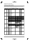
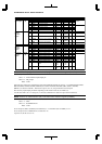
III PERIPHERAL BLOCK: SERIAL INTERFACE
B-III-8-32 EPSON S1C33L03 FUNCTION PART
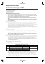
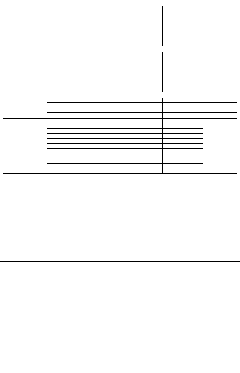
NameAddressRegister name Bit Function Setting Init. R/W Remarks
CFP07
CFP06
CFP05
CFP04
CFP03
CFP02
CFP01
CFP00
D7
D6
D5
D4
D3
D2
D1
D0
P07 function selection
P06 function selection
P05 function selection
P04 function selection
P03 function selection
P02 function selection
P01 function selection
P00 function selection
0
0
0
0
0
0
0
0
R/W
R/W
R/W
R/W
R/W
R/W
R/W
R/W
Extended functions
(0x402DF)
00402D0
(B)
1 #SRDY1 0 P07
1 #SCLK1 0 P06
1 SOUT1 0 P05
1 SIN1 0 P04
1 #SRDY0 0 P03
1 #SCLK0 0 P02
1 SOUT0 0 P01
1 SIN0 0 P00
P0 function
select register
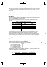
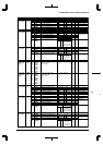
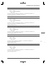
–
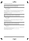
SSRDY3
SSCLK3
SSOUT3
SSIN3
D7–4
D3
D2
D1
D0
reserved
Serial I/F Ch.3 SRDY selection
Serial I/F Ch.3 SCLK selection
Serial I/F Ch.3 SOUT selection
Serial I/F Ch.3 SIN selection
– –
0
0
0
0
–
R/W
R/W
R/W
R/W
00402D7Port SIO
function
extension
register
1 #SRDY3 0
P32/
#DMAACK0
1 #SCLK3 0
P15/EXCL4/
#DMAEND0
1 SOUT3 0
P16/EXCL5/
#DMAEND1
1 SIN3 0
P33/
#DMAACK1
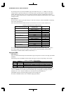
–
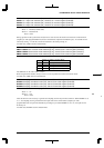
SSRDY2
SSCLK2
SSOUT2
SSIN2
D7–4
D3
D2
D1
D0
reserved
Serial I/F Ch.2 SRDY selection
Serial I/F Ch.2 SCLK selection
Serial I/F Ch.2 SOUT selection
Serial I/F Ch.2 SIN selection
–
0
0
0
0
–
R/W
R/W
R/W
R/W
00402DB
1 #SRDY2 0 P24/TM2
1 #SCLK2 0 P25/TM3
1 SOUT2 0 P26/TM4
1 SIN2 0 P27/TM5
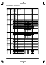
Port SIO
function
extension
register
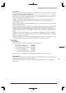
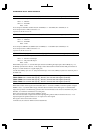
–
CFEX7
CFEX6
CFEX5
CFEX4
CFEX3
CFEX2
CFEX1
CFEX0
D7
D6
D5
D4
D3
D2
D1
D0
P07 port extended function
P06 port extended function
P05 port extended function
P04 port extended function
P31 port extended function
P21 port extended function
P10, P11, P13 port extended
function
P12, P14 port extended function
0
0
0
0
0
0
1
1
R/W
R/W
R/W
R/W
R/W
R/W
R/W
R/W
00402DF
(B)
Port function
extension
register
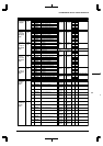
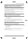
1
#DMAEND3
0 P07, etc.
1
#DMAACK3
0 P06, etc.
1
#DMAEND2
0 P05, etc.
1
#DMAACK2
0 P04, etc.
1 #GARD 0 P31, etc.
1 #GAAS 0 P21, etc.
1 DST0
DST1
DPC0
0 P10, etc.
P11, etc.
P13, etc.
1 DST2
DCLK
0 P12, etc.
P14, etc.
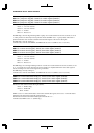
CFP07–CFP00: P0[7:0] pin function selection (D[7:0]) / P0 function select register (0x402D0)
Selects the pins used for the serial interface.
Write "1": Serial-interface input/output pin
Write "0": I/O port pin
Read: Valid
Select the pins used for the serial interface from among P00 through P07 by writing "1" to CFP00 through CFP07.
P00–P03 (SIN0, SOUT0, #SCLK0, #SRDY0) are used for channel 0; P04–P07 (SIN1, SOUT1, #SCLK1,
#SRDY1) are used for channel 1. If the bit for a pin is set to "0", the pin functions as an I/O port.
The necessary input/output pins differ depending on the transfer mode set (see Table 8.3).
At cold start, CFP is set to "0" (I/O port). At hot start, CFP retains its state from prior to the initial reset.
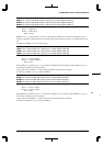
SSIN3: Serial I/F Ch.3 SIN selection (D0) / Port SIO function extension register (0x402D7)
Switches the function of pin P33/#DMAACK1/SIN3.
Write "1": SIN3
Write "0": P33/#DMAACK1
Read: Valid
To use the pin as SIN3, set SSIN3 (D0 / 0x402D7) to "1" and CFP33 (D3 / 0x402DC) to "0".
To use the pin as P33 or #DMAACK1, set this bit to "0".
At power-on, this bit is set to "0".