


II CORE BLOCK: BCU (Bus Control Unit)
S1C33L03 FUNCTION PART EPSON B-II-4-3
A-1
B-II
BCU
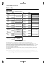
Combination of System Bus Control Signals
The bus control signal pins that have two or more functions have their functionality determined when an interface
method is selected by a program. The BCU contains an ordinary external system interface (two interface method
are supported) and a DRAM interface.
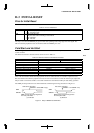
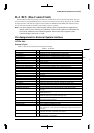
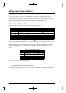
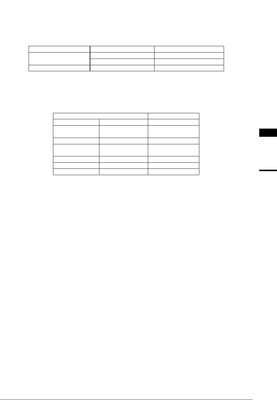
Table 4.3 Interface Selection
Interface type Interface method Control bit
External system interface A0 system (default) SBUSST(D3/0x4812E) = "0"
#BSL system SBUSST(D3/0x4812E) = "1"
DRAM interface 2CAS system (fixed) None
SBUSST is initialized to "0" at cold start.
When the IC is hot-started, these bits retain their status before the chip was reset.
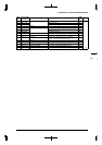
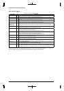
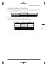
Table 4.4 shows combinations of control signals classified by each interface method.
Table 4.4 Combinations of Bus Control Signals
External system interface DRAM interface
A0 system #BSL system 2CAS system
A0 #BSL (little endian) /
#BSH (big endian) ∗1
–
#WRL #WR #WE
#WRH #BSH (little endian) /
#BSL (big endian) ∗1
–
––#HCAS
––#LCAS
#CEx #CEx #RASx ∗2
∗1In the #BSL system, the A0 and #WRH pin functions change according to the endian selected (little endian
or big endian).
∗2 When using DRAM, the #CE output pins in areas 7–8 (areas 13–14) function as the #RAS1–2 (#RAS3–4)
pins.