


APPENDIX A <REFERENCE> EXTERNAL DEVICE INTERFACE TIMINGS
S1C33L03 PRODUCT PART EPSON A-127
A-1
A-ap
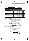
A.6 8255A
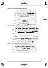
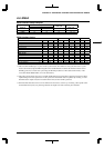
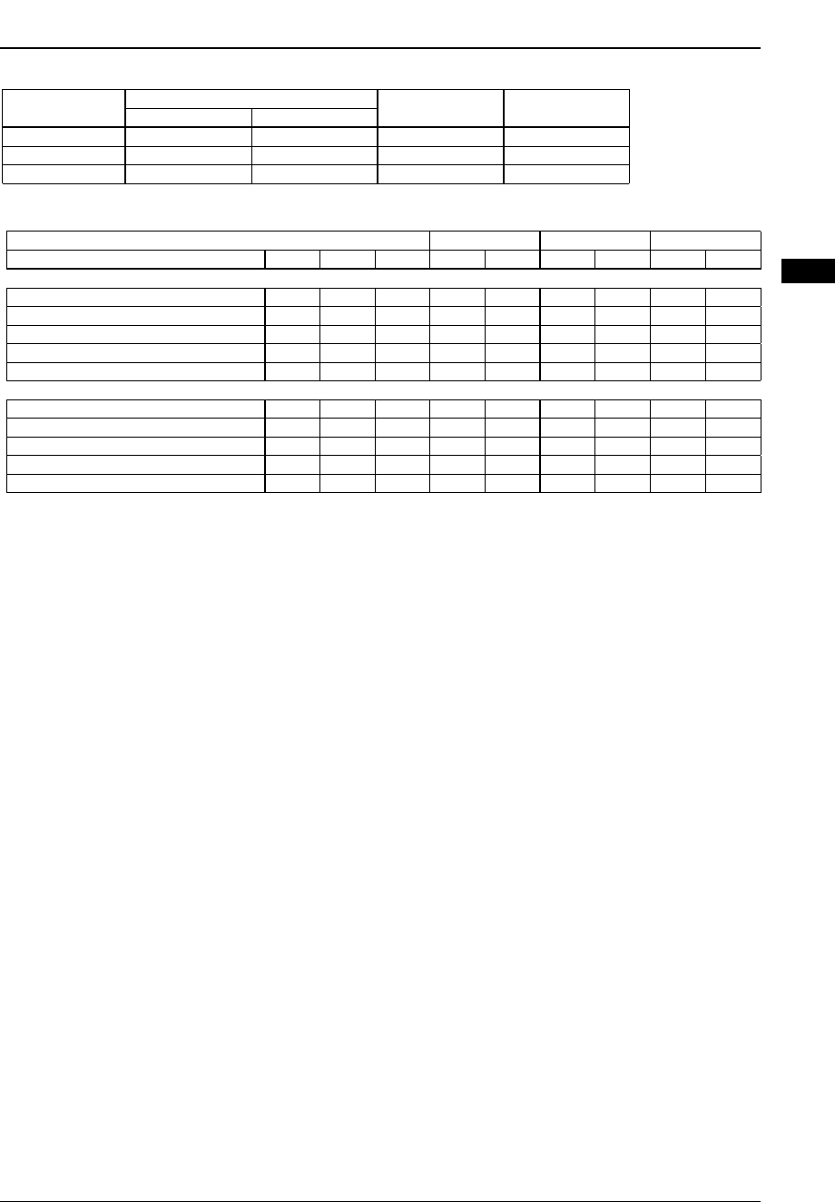
8255A interface setup examples
Operating Read cycle Output disable
frequency Wait cycle Read cycle
Write cycle
delay cycle
20MHz 9 ∗110 10 3.5
25MHz 11 12 12 3.5
33MHz 14 15 15 3.5 ∗2
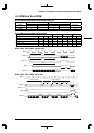
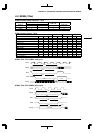
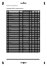
8255A interface timing
SRAM interface 33MHz 25MHz 20MHz
Parameter Symbol Min. Max. Cycle Time Cycle Time Cycle Time
<Read cycle>
Read cycle time tRC 300 – 15 450 12 480 10 500
Address access time tACC –25015450 12 480 10 500
#CE access time tACS –25015450 12 480 10 500
#OE access time tOE –25014.5435 11.5460 9.5475
Output disable delay time tOHZ 10 150 3.5 105 3.5 140 3.5 175
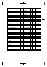
<Write cycle>
Write cycle time tWC 430 – 15 450 12 480 10 500
Address enable time tAW 400 – 14.5 435 11.5 460 9.5 475
Write pulse width tWP 400 – 14 420 11 440 9 450
Input data setup time tDW 100 – 14 420 11 440 9 450
Input data hold time ∗3 tDH 30 – 0.5 15 0.5 20 0.5 25
∗1The S1C33L03 enables up to 7 cycles of wait-cycle insertion. If a number of wait cycles more than 7 cycles
needs to be inserted, input the #WAIT signal from external hardware. Note that the interface must be set for
SRAM type devices to insert wait cycles using the #WAIT pin. (Refer to "BCU (Bus Control Unit)" in the
"S1C33L03 FUNCTION PART", for more information.)
∗2This setting cannot satisfy the 150 ns of output-disable delay time specification required for the 8255A. When
implementing such a low-speed device in the system, the external bus must be separated by inserting a 3-state
bus buffer at the output side (when viewed from the CPU) of the external system bus.
∗3If the data hold time that can be set is not sufficient for the device, secure it by connecting a bus repeater to the
external data bus D[15:0] or by inserting a latch at the output side of the external system interface.