


1 OUTLINE
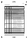
A-6 EPSON S1C33L03 PRODUCT PART
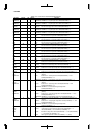
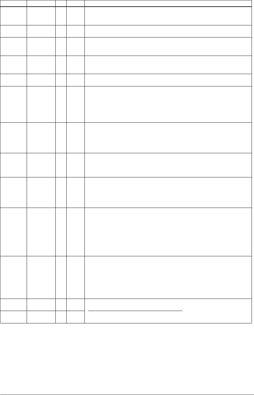
Pin name Pin No. I/O Pull-up Function
#WRL
#WR
#WE
43 O – #WRL: Write (low byte) signal when SBUSST(D3/0x4812E) = "0" (default)
#WR: Write signal when SBUSST(D3/0x4812E) = "1"
#WE: DRAM write signal
#WRH
#BSH
42 O – #WRH: Write (high byte) signal when SBUSST(D3/0x4812E) = "0" (default)
#BSH: Bus strobe (high byte) signal when SBUSST(D3/0x4812E) = "1"
#HCAS
#SDCAS
77 O – #HCAS: DRAM column address strobe (high byte) signal when
SDRENA(D7/0x39FFC1) = "0" (default)
#SDCAS: SDRAM column address strobe when SDRENA(D7/0x39FFC1) = "1"
#LCAS
#SDRAS
76 O – #LCAS: DRAM column address strobe (low byte) signal when
SDRENA(D7/0x39FFC1) = "0" (default)
#SDRAS: SDRAM row address strobe when SDRENA(D7/0x39FFC1) = "1"
BCLK
SDCLK
81 O – BCLK: Bus clock output when SDRENA(D7/0x39FFC1) = "0" (default)
SDCLK: SDRAM clock output when SDRENA(D7/0x39FFC1) = "1"
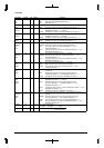
P34
#BUSREQ
#CE6
GPIO0
71 I/O – P34: I/O port when CFP34(D4/0x402DC) = "0" (default)
#BUSREQ: Bus release request input when CFP34(D4/0x402DC) = "1"
#CE6: Area 6 chip enable when CFP34(D4/0x402DC) = "1" and
IOC34(D4/0x402DE) = "1"
GPIO0: LCDC general-purpose I/O when LCDCEN(D5/0x39FFE3) = "1" and
BREQEN(D2/0x39FFFD) = "0"
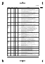
P35
#BUSACK
GPIO1
70 I/O – P35: I/O port when CFP35(D5/0x402DC) = "0" (default)
#BUSACK: Bus acknowledge output when CFP35(D5/0x402DC) = "1" and
CFP34(D4/0x402DC) = "1"
GPIO1: LCDC general-purpose I/O when LCDCEN(D5/0x39FFE3) = "1" and
BREQEN(D2/0x39FFFD) = "0"
P30
#WAIT
#CE4&5
75 I/O – P30: I/O port when CFP30(D0/0x402DC) = "0" (default)
#WAIT: Wait cycle request input when CFP30(D0/0x402DC) = "1"
#CE4&5: Areas 4&5 chip enable when CFP30(D0/0x402DC) = "1" and
IOC30(D0/0x402DE) = "1"
P20
#DRD
SDCKE
80 I/O – P20: I/O port when CFP20(D0/0x402D8) = "0" and SDRENA(D7/0x39FFC1) =
"0" (default)
#DRD: DRAM read signal output for successive RAS mode when
CFP20(D0/0x402D8) = "1" and SDRENA(D7/0x39FFC1) = "0"
SDCKE: SDRAM clock enable signal when SDRENA(D7/0x39FFC1) = "1"
P21
#DWE
#GAAS
#SDWE
79 I/O – P21: I/O port when CFP21(D1/0x402D8) = "0", CFEX2(D2/0x402DF) = "0" and
SDRENA(D7/0x39FFC1) = "0" (default)
#DWE: DRAM write signal output for successive RAS mode when
CFP21(D1/0x402D8) = "1", CFEX2(D2/0x402DF) = "0" and
SDRENA(D7/0x39FFC1) = "0"
#GAAS: Area address strobe output for GA when CFEX2(D2/0x402DF) = "1" and
SDRENA(D7/0x39FFC1) = "0"
#SDWE: SDRAM write signal when SDRENA(D7/0x39FFC1) = "1"
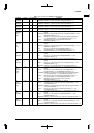
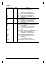
P31
#BUSGET
#GARD
GPIO2
74 I/O – P31: I/O port when CFP31(D1/0x402DC) = "0" and CFEX3(D3/0x402DF) = "0"
(default)
#BUSGET: Bus status monitor signal output for bus release request when
CFP31(D1/0x402DC) = "1" and CFEX3(D3/0x402DF) = "0"
#GARD: Area read signal output for GA when CFEX3(D3/0x402DF) = "1"
GPIO2: LCDC general-purpose I/O when LCDCEN(D5/0x39FFE3) = "1" and
BREQEN(D2/0x39FFFD) = "0"
EA10MD1 123 I Pull-up Area 10 boot mode selection
EA10MD1 EA10MD0 Mode
EA10MD0 124 I – 1 1 External ROM mode
10Internal ROM mode