


VII LCD CONTROLLER BLOCK: LCD CONTROLLER
B-VII-2-40 EPSON S1C33L03 FUNCTION PART
PMODSEL: Portrait mode select (D6) / Portrait mode register (0x39FFFB)
Selects a type of portrait mode.
Write "1": Alternate portrait mode
Write "0": Default portrait mode
Read: Valid
Setting PMODSEL to "1" selects alternate portrait mode, and setting PMODSEL to "0" selects default portrait
mode. When PMODEN (D7/0x39FFFB) is set to "1", data is displayed in the selected portrait mode. For details,
refer to "Portrait Mode".
At initial reset, PMODSEL is set to "0" (default portrait mode).
PMODCLK[1:0]: Portrait mode clock select (D[1:0]) / Portrait mode register (0x39FFFB)
Selects the clock used in portrait mode.
In alternate portrait mode, the MCLK clock used for display memory access must be twice as fast as the pixel clock,
PCLK. Therefore, clock settings differ between the alternate and default portrait modes.
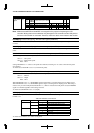
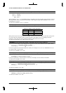
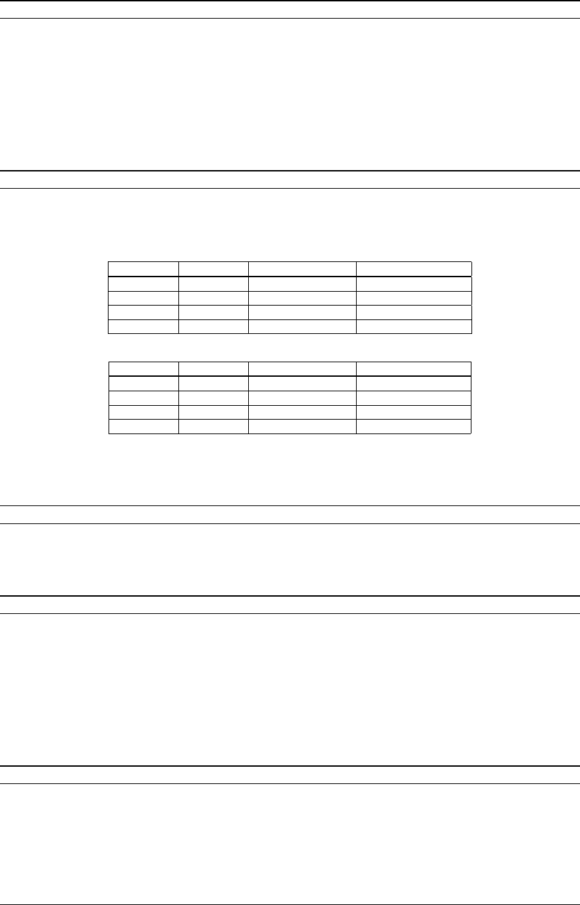
Table 2.26 Clock Settings for Default Portrait Mode
PMODCLK1 PMODCLK0 Pixel clock PCLK Memory clock MCLK
00 CLK CLK
01 CLK/2 CLK/2
10 CLK/4 CLK/4
11 CLK/8 CLK/8
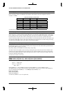
Table 2.27 Clock Settings for Alternate Portrait Mode
PMODCLK1 PMODCLK0 Pixel clock PCLK Memory clock MCLK
00 CLK/2 CLK
01 CLK/2 CLK
10 CLK/4 CLK/2
11 CLK/8 CLK/4
CLK denotes the clock for landscape mode (PCLK = MCLK), which is selected by LCLKSEL[2:0]
(D[2:0]/0x39FFF4).
At initial reset, PMODCLK is set to "0b00".
PMODLBC[7:0]: Line byte count (D[7:0]) / Line byte count register (0x39FFFC)
Sets the number of bytes equivalent to one line in portrait mode. For this line byte count, write the number of
horizontal pixels converted into the number of bytes available in bpp mode. These horizontal pixels include the
number of pixels in a virtual portion of the screen that is not displayed on the LCD panel.
At initial reset, PMODLBC is set to "0x0".
VRAMAR: VRAM area select (D7) / LCDC system control register (0x39FFFD)
Selects the area in which the display memory is located.
Write "1": Area 8 (or 14)
Write "0": Area 7 (or 13)
Read: Valid
Setting VRAMAR to "1" selects area 8 (when CEFUNC[1:0] (D[A:9]/0x48130) = "0b00") or area 14 (when
CEFUNC = "0b01"), and setting VRAMAR to "0" selects area 7 (when CEFUNC = "0b00") or area 13 (when
CEFUNC = "0b01").
At initial reset, VRAMAR is set to "0" (area 7).
VRAMWT[2:0]: VRAM wait control (D[6:4]) / LCDC system control register (0x39FFFD)
Sets the number of wait cycles (0–7) for display memory access.
This setting is effective only when SRAM is used for the display memory. Settings of this register are ignored
when SDRAM is used. The number of wait cycles set here is inserted when the LCD controller accesses the
display memory. It does not affect display-memory access by the CPU. In that case, the number of wait cycles set
for the BCU is inserted.
At initial reset, VRAMWT is set to "0x0".