


8 ELECTRICAL CHARACTERISTICS
S1C33L03 PRODUCT PART EPSON A-79
A-1
A-8
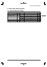
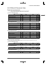
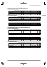
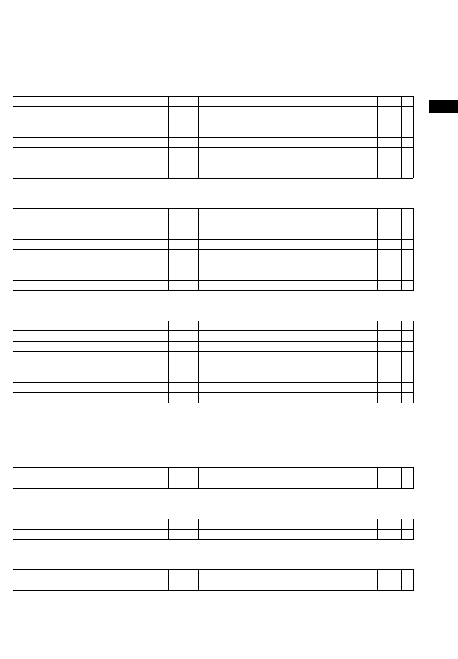
8.6.3 C33 Block AC Characteristic Tables
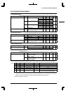
External clock input characteristics
(Note) These AC characteristics apply to input signals from outside the IC.
The OSC3 input clock must be within V
DD to VSS voltage range.
1) 3.3 V/5.0 V dual power source
(Unless otherwise specified: VDDE=5.0V±0.5V, VDD=2.7V to 3.6V, VSS=0V, Ta=-40°C to +85°C)
Item Symbol Min. Max. Unit ∗
High-speed clock cycle time tC3 30 ns
OSC3 clock input duty tC3ED 45 55 %
OSC3 clock input rise time tIF 5ns
OSC3 clock input fall time tIR 5ns
BCLK high-level output delay time tCD1 35 ns
BCLK low-level output delay time tCD2 35 ns
Minimum reset pulse width tRST 6·tCYC ns
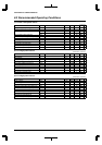
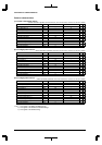
2) 3.3 V single power source
(Unless otherwise specified: VDDE=VDD=2.7V to 3.6V, VSS=0V, Ta=-40°C to +85°C)
Item Symbol Min. Max. Unit ∗
High-speed clock cycle time tC3 30 ns
OSC3 clock input duty tC3ED 45 55 %
OSC3 clock input rise time tIF 5ns
OSC3 clock input fall time tIR 5ns
BCLK high-level output delay time tCD1 35 ns
BCLK low-level output delay time tCD2 35 ns
Minimum reset pulse width tRST 6·tCYC ns
3) 2.0 V single power source
(Unless otherwise specified: VDDE=VDD=2.0V±0.2V, VSS=0V, Ta=-40°C to +85°C)
Item Symbol Min. Max. Unit ∗
High-speed clock cycle time tC3 50 ns
OSC3 clock input duty tC3ED 45 55 %
OSC3 clock input rise time tIF 5ns
OSC3 clock input fall time tIR 5ns
BCLK high-level output delay time tCD1 60 ns
BCLK low-level output delay time tCD2 60 ns
Minimum reset pulse width tRST 6·tCYC ns
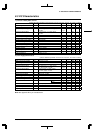
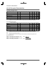
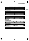
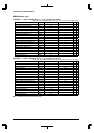
BCLK clock output characteristics
(Note) These AC characteristic values are applied only when the high-speed oscillation circuit is used.
1) 3.3 V/5.0 V dual power source
(Unless otherwise specified: VDDE=5.0V±0.5V, VDD=2.7V to 3.6V, VSS=0V, Ta=-40°C to +85°C)
Item Symbol Min. Max. Unit ∗
BCLK clock output duty tCBD 40 60 %
2) 3.3 V single power source
(Unless otherwise specified: VDDE=VDD=2.7V to 3.6V, VSS=0V, Ta=-40°C to +85°C)
Item Symbol Min. Max. Unit ∗
BCLK clock output duty tCBD 40 60 %
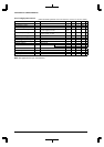
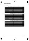
3) 2.0 V single power source
(Unless otherwise specified: VDDE=VDD=2.0V±0.2V, VSS=0V, Ta=-40°C to +85°C)
Item Symbol Min. Max. Unit ∗
BCLK clock output duty tCBD 40 60 %