


94
CHAPTER 5 CLOCKS
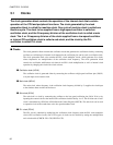
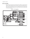
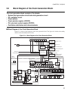
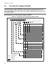
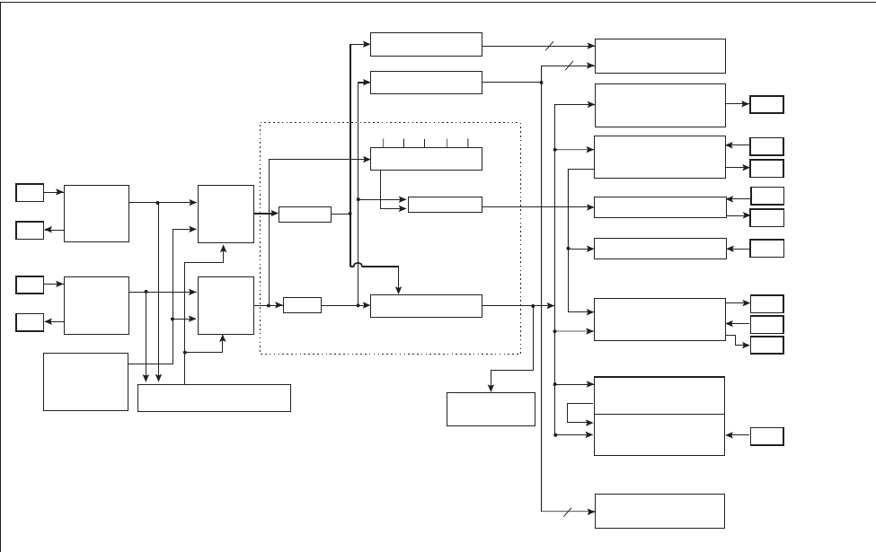
■ Clock Supply Map
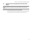
Since the machine clock generated in the clock generation block is supplied as the clock that controls the
operation of the CPU and peripheral functions, the operation of the CPU and the peripheral functions is
affected by switching between the main clock, the PLL clock and the subclock (clock mode) and by a
change in the PLL clock multiplication ratio. Since some peripheral functions receive frequency-divided
output from the timebase timer, a peripheral unit can select the clock best suited for this operation. Figure
5.1-1 shows the clock supply map.
Figure 5.1-1 Clock Supply Map
Timebase timer
Clock selector
8/16-bit
PPG timer C to F
16-bit
reload timer 2, 3
CAN1
Oscillation stabilization
wait control
Watchdog timer
Clock
generator
Pin
Pin
X1
X0
X1A
X0A
HCLK
(oscillation clock)
SCLK (sub clock)
Pin
TIN2, TIN3
Clock control
block
Peripheral function
HCLK : Oscillation clock
MCLK : Main clock
PCLK : PLL clock
SCLK : Sub clock
f : Machine clock
f
c
: CAN0 to CAN2 clock
2-divided
4/2-divided
CPU
Pin
PPGC to F
f
(machine clock)
f
c
4
4
Watch timer
Pin
TOT0 to 3
Clock
generator
Pin
Pin
4
Pin
RX1
Pin
TX1
PLL multiplication circuit
123
PCLK(PLL clock)
4
6
Clock selector
A/D converter (16ch)
Pin
AN0 to AN15
UART0 to 1+
serial I/O
Pin
SIN0, SIN1
Pin
SCK0, SCK1
Pin
SOT0, SOT1
Pin
IN0 to IN3
I/O timer
Free-run timer 0,1
Input capture 0 to 3
Clock
selector
Clock
selector
Internal
CR oscillation
clock
Clock supervisor function