637
APPENDIX C Timing Diagrams in Flash Memory Mode
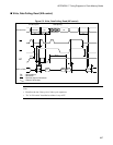
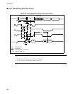
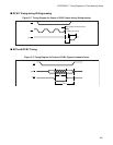
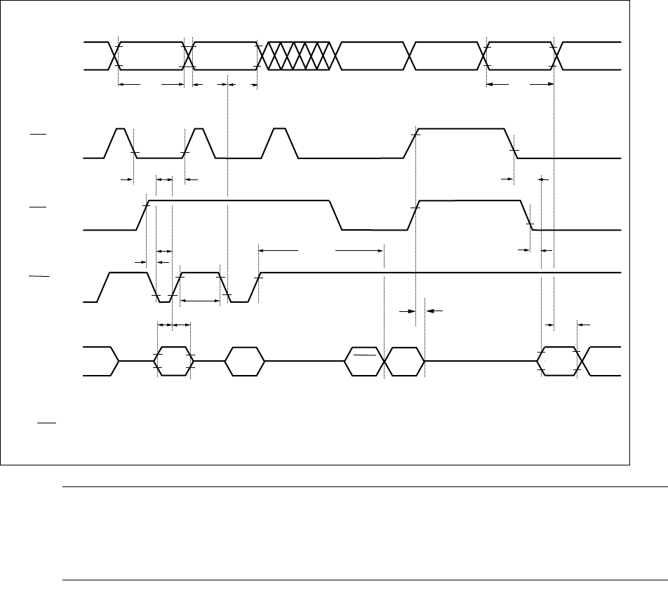
■ Write, Data Polling, Read (WE control)
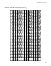
Figure C-2 Write, Data Polling, Read (WE control)
Note:
• Describes the last 2-bus cycle of 4-bus cycle sequences.
• "Fx" in "FxAAAA" described as address is any of FF.
tCH
tCS
tWP
tWHWH1
tWC
CE
OE
tRC
AQ18
to
AQ0
DQ7
to
DQ0
tGHWL
tCE
tOE
tWPH
tDS
tDH
DQ7
PD
A0
H
DOUT DOUT
WE
FxAAAAH
PA PA
tOH
t
AS
tAH
tDF
PA : Write address
PD : Write data
DQ
7
: Reverse output of write data
D
OUT
: Output of write data
3rd bus cycle
Data polling


