


427
CHAPTER 20 LIN-UART
●
Clock supply:
In operation mode 2, the number of clock cycles for the clock signal must be the same as the number of bits
for the transmission and reception. If the start/stop bits are enabled, it must be matched the additional start/
stop bits. If the MS bit of the ECCR register is "0" (master mode) and the SCKE bit of the SMR register is
"1" (serial clock output enabled), the consistent clock cycles are generated automatically. If the MS bit of
the ECCR register is "1" (slave mode), or if the SCKE bit of SMR is 0 (serial clock output disabled), the
clock for each bit of transfer data must be supplied from outside. While there is no communication, the
clock signal must be kept at "H" as the mark level
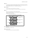
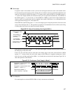
If the SCDE bit of the ECCR register is "1", the clock output signal is delayed by the half of the serial clock
cycle as shown in Figure 20.7-5 . The operation is prepared for communication devices which use the rising
or falling edge of the serial clock signal for the data sampling.
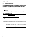
Figure 20.7-5 Delayed Transmitting Clock Signal(SCDE=1)
If the SCES bit of the ESCR register is "1", the serial clock signal is inverted. Receiving data is sampled at
the falling edge of the serial clock.
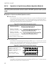
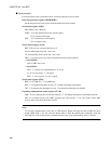
In this case, the serial data must be valid value at the falling edge of the clock. If the CCO bit of ESCR
register is "1" (master mode), the serial clock output of the SCKn pin is supplied continuously. In this
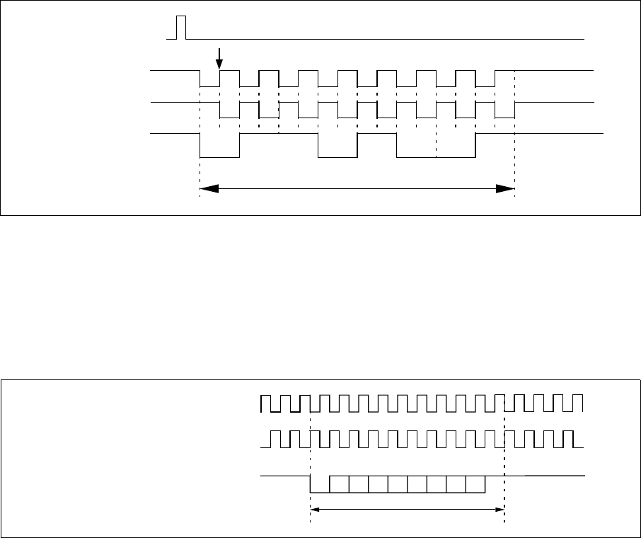
mode, be sure to add the start/stop bits (SSM = 1) to identify the start and end of data frame. Figure 20.7-6
shows the operation of this function.
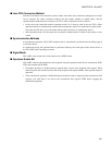
Figure 20.7-6 Continuous Clock Supply in Mode 2
●
Error detection:
If no start/stop bits are selected (ECCR: SSM = 0) only overrun errors are detected.
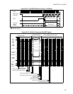
Transmission data
writing
Transmitting or
receiving clock
Transmission and
reception data
1
Data
LSB MSB
Mark level
(normal)
Transmitting
clock (SCDE = 1)
Mark level
Mark level
Reception data sample edge (SCES = 0)
0110100
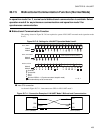
data frame
Reception or transmission clock
Data stream (SSM = 1)
(here: no parity, 1 stop bit)
ST SP
(SCES = 0, CCO = 1):
Reception or transmission clock
(SCES = 1, CCO = 1):