531
CHAPTER 24 512K-BIT FLASH MEMORY
24.2 Block Diagram of the Entire Flash Memory and Sector
Configuration of the Flash Memory
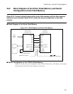
Figure 24.2-1 shows a block diagram of the entire flash memory with the flash memory
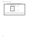
interface circuit included. Figure 24.2-2 shows the sector configuration of the flash
memory.
■ Block Diagram of the Entire Flash Memory
Figure 24.2-1 Block Diagram of the Entire Flash Memory
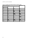
■ Sector Configuration of the 512K-bit Flash Memory
Figure 24.2-2 shows the sector configuration of the 512K-bit flash memory. The addresses in the figure
indicate the high-order and low-order addresses of each sector.
BYTE
CE
OE
WE
AQ0 to AQ18
DQ0 to DQ15
RY/BY
BYTE
CE
OE
WE
AQ0 to AQ15
AQ
-1
DQ0 to DQ15
RY/BY
INT
RESET
RY/BY
Flash memory
interface circuit
Write enable signal
512K bits
flash memory
Write enable interrupt
signal (to CPU)
External reset signal
F
2
MC-16LX
bus
Port 2
Port 4
Port 5


