


539
CHAPTER 24 512K-BIT FLASH MEMORY
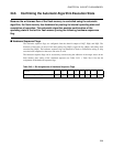
24.6 Confirming the Automatic Algorithm Execution State
Because the write/erase flow of the flash memory is controlled using the automatic
algorithm, the flash memory has hardware for posting its internal operating state and
completion of operation. This automatic algorithm enables confirmation of the
operating state of the built-in flash memory using the following hardware sequences
flag.
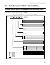
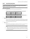
■ Hardware Sequence Flags
The hardware sequence flags are configured from the three-bit output of DQ7, DQ6, and DQ5. The
functions of these bits are those of the data polling flag (DQ7), toggle bit flag (DQ6), and timing limit
exceeded flag (DQ5). The hardware sequence flags can therefore be used to confirm that writing or chip
erase has been completed or that erase code write is valid.
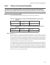
The hardware sequence flags can be accessed by read-accessing the addresses of the target sectors in the
flash memory after setting of the command sequence (see Table 24.5-1 ). Table 24.6-1 lists the bit
assignments of the hardware sequence flags.
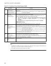
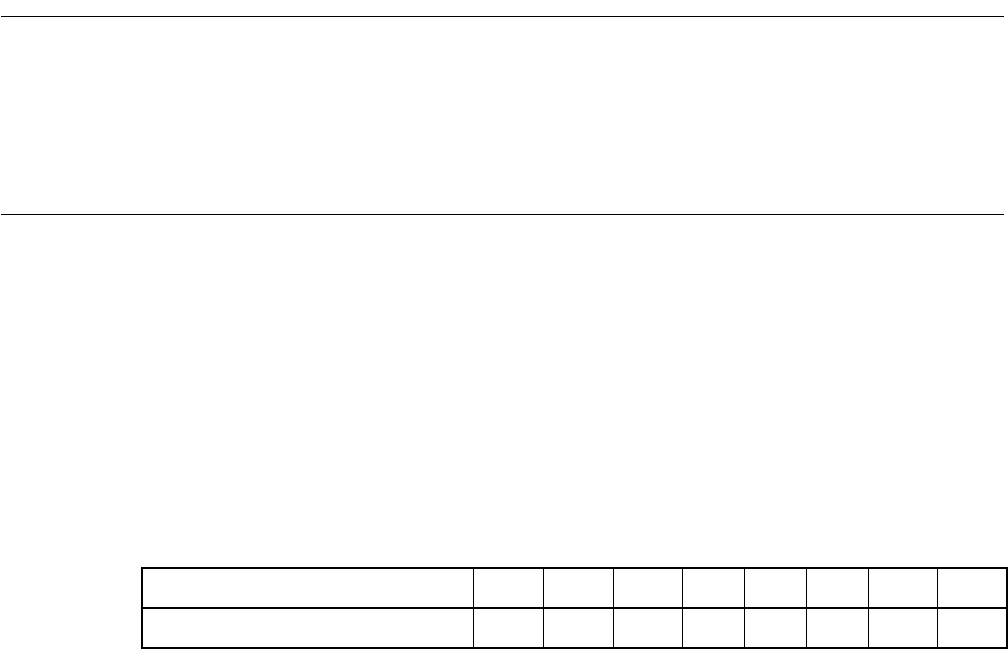
Table 24.6-1 Bit Assignments of Hardware Sequence Flags
Bit No. 7 6 5 4 3 2 1 0
Hardware sequence flag DQ7 DQ6 DQ5 − − − − −