43
CHAPTER 2 CPU
●
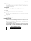
T: Sticky bit flag:
1 is set in the T flag when there is at least one "1" in the data shifted out from the carry after execution of a
logical right/arithmetic right shift instruction. Otherwise, 0 is set in the T flag. In addition, "0" is set in the
T flag when the shift amount is zero.
●
N: Negative flag:
The N flag is set when the MSB of the operation result is "1", and is otherwise cleared.
●
Z: Zero flag:
The Z flag is set when the operation result is all zeroes, and is otherwise cleared.
●
V: Overflow flag:
The V flag is set when an overflow of a signed value occurs as a result of operation execution and is
otherwise cleared.
●
C: Carry flag:
The C flag is set when a carry-up or carry-down from the MSB occurs as a result of operation execution,
and is otherwise cleared.
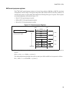
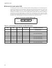
■ Register Bank Pointer (RP)
The RP register indicates the relationship between the general-purpose registers of the F
2
MC-16LX and the
internal RAM addresses. Specifically, the RP register indicates the first memory address of the currently
used register bank in the following conversion expression: [00180
H
+ (RP)*10
H
] (see Figure 2.7-8 ). The
RP register consists of five bits, and can take a value between 00
H
and 1F
H
. Register banks can be allocated
at addresses from 000180
H
to 00037
H
in memory.
Even within that range, however, the register banks cannot be used as general-purpose registers if the banks
are not in internal RAM. The RP register is initialized to all zeroes by a reset. An instruction may transfer
an eight-bit immediate value to the RP register; however, only the low-order five bits of that data are used.
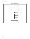
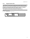
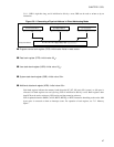
Figure 2.7-8 Register Bank Pointer (RP)
B4 B3 B2 B1 B0 : RP
Initial value 0 0 0 0 0


