462
CHAPTER 21 CAN CONTROLLER
21.4.7 Bit Timing Register (BTR)
Bit timing register (BTR) sets the prescaler and bit timing setting.
■ Register Configuration
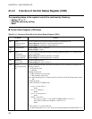
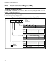
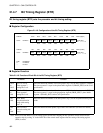
Figure 21.4-6 Configuration of the Bit Timing Register (BTR)
■ Register Function
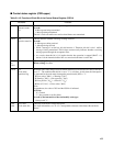
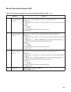
Table 21.4-6 Function of Each Bit of the Bit Timing Register (BTR)
Bit Name Function
bit14
to
bit12
TS2.2 to TS2.0:
Time segment 2
setting bits 2 to 0
These bits define the number of the time quanta (TQ’s) for the time segment 2 (TSEG2).
The time segment 2 is equal to the phase buffer segment 2 (PHASE_SEG2) in the CAN
specification.
bit11
to
bit8
TS1.3 to TS1.0:
Time segment 1
setting bits 3 to 0
These bits define the number of the time quanta (TQ’s) for the time segment 1 (TSEG1).
The time segment 1 is equal to the propagation segment (PROP_SEG) + phase buffer
segment 1 (PHASE_SEG1) in the CAN specification.
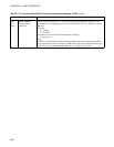
bit7
bit6
RSJ1, RSJ0:
Resynchronization
jump width setting
bits 1, 0
These bits define the number of the time quanta (TQ’s) for the resynchronization jump
width.
bit5
to
bit0
PSC5 to PSC0:
Prescaler setting bits
5 to 0
These bits define the time quanta (TQ) of the CAN controller. (see below for details.)
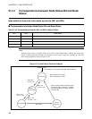
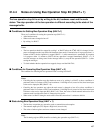
Note: Please set (CSR: HALT=1) to bit timing register (BTR) after stopping the bus operation. Please release the bus
operation stop by writing "0" in the HALT bit of the control status register after the setting of bit timing register
(BTR) is ended.
Address bit15 bit14 bit13 bit12 bit11 bit10 bit9 bit8 BTR1(Upper)
CAN1: 007D07
H − TS2.2 TS2.1 TS2.0 TS1.3 TS1.2 TS1.1 TS1.0 Reset value
X1 1 1 1 1 1 1
B
− R/W R/W R/W R/W R/W R/W R/W
Address bit7 bit6 bit5 bit4 bit3 bit2 bit1 bit0 BTR1(Lower)
CAN1: 007D06
H
RSJ1 RSJ0 PSC5 PSC4 PSC3 PSC2 PSC1 PSC0 Reset value
11 1 1 1 1 1 1
B
R/WR/WR/WR/WR/WR/WR/WR/W
R/W :
X :
− :
Read/Write
Undefined
Unused


