530
CHAPTER 24 512K-BIT FLASH MEMORY
24.1 Overview of 512K-bit Flash Memory
The 512K-bit flash memory is mapped to the FF
H
bank in the CPU memory map. The
functions of the flash memory interface circuit enable read-access and program-access
from the CPU in the same way as mask ROM. Instructions from the CPU can be used via
the flash memory interface circuit to write data to and erase data from the flash memory.
Internal CPU control therefore enables rewriting of the flash memory while it is
mounted. As a result, improvements in programs and data can be performed efficiently.
■ 512K-bit Flash Memory Features
• Use of automatic program algorithm (Embedded Algorithm
TM*
: Equivalent to MBM29LV200)
• Detection of completion of writing/erasing using data polling or toggle bit functions
• Detection of completion of writing/erasing using CPU interrupts
• Minimum of 10,000 write/erase operations
• Flash reading cycle time: Minimum of 2 machine cycles
*: Embedded Algorithm
TM
is a trademark of Advanced Micro Devices, Inc.
Note:
The manufacturer code and device code do not have the reading function. These codes cannot be
accessed by the command.
■ Writing to/erasing Flash Memory
The flash memory cannot be written to and erased at the same time. That is, when data is written to or
erased data from the flash memory, the program in the flash memory must first be copied to RAM. The
entire process is then executed in RAM so that data is simply written to the flash memory. This eliminates
the need for the program to access the flash memory from the flash memory itself.
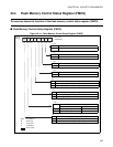
■ Flash Memory Control Status Register (FMCS)
Figure 24.1-1 Flash Memory Control Status Register (FMCS)
7654321
0
(R/W) (R/W) (R/W) (R)
INTE
RDYINT WE RDY
(0) (0) (0) (X) (0) (0) (0) (0)
FMCS
0000AEH
(R/W) (R/W)(R/W)(R/W)
Flash memory control status register (FMCS)
Address:
Read/Write
Initial value
Reserved Reserved Reserved Reserved
R/W: Read/Write
R : Read only


