401
CHAPTER 20 LIN-UART
20.4.5 Extended Status/Control Register (ESCR)
This register provides several LIN functions, direct access to the SINn and SOTn pins
and setting of continuous clock output and sampling clock edge in LIN-UART
synchronous clock mode.
■ Extended Status/control Register (ESCR)
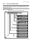
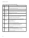
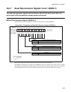
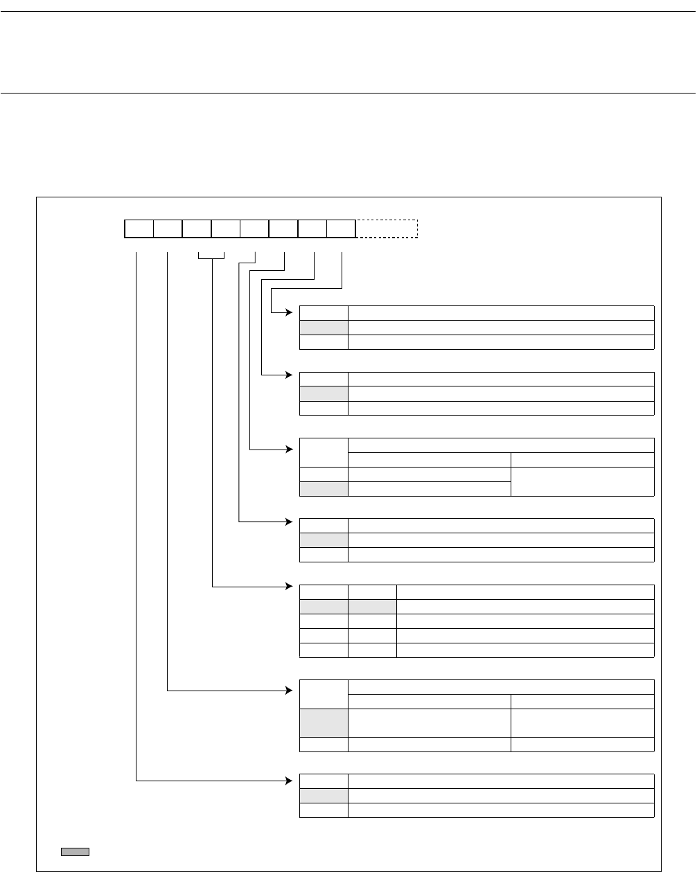
Figure 20.4-6 shows the Configuration of the extended status/control register (ESCR), and Table 20.4-4
shows the function of each bit.
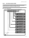
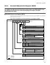
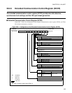
Figure 20.4-6 Configuration of the Extended Status/control Register (ESCR)
LBIE LBD LBL1 LBL0 SIOP CCO SCES
00000100
B
SOPE
ESCR0 : 000025H
ESCR1 : 00002DH
bit 15 bit 14 bit 13 bit 12 bit 11 bit 10 bit 9 bit 8
R/W R/W R/W R/W R/W R/W R/W R/W
bit 7 bit 0
Address
Initial value
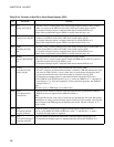
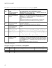
bit 8
SCES Sampling Clock Edge Selection Bit (Mode 2)
0 Sampling on rising clock edge (normal)
1 Sampling on falling clock edge (inverted clock)
bit 9
CCO Continuous Clock Output Enable Bit (Mode 2)
0 Continuous Clock Output disabled
1 Continuous Clock Output enabled
bit 10
SIOP
Serial Input/Output Pin Access
write (SOPE = "1") read
0 SOTn pin is forced to "0"
Reading the actual value of
SINn pin
1 SOTn pin is forced to "1"
bit 11
SOPE Serial Output pin direct Access Enable Bit
0 Serial Output pin direct access disable
1 Serial Output pin direct access enable
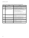
bit 12 bit 13
LBL0 LBL1 LIN Synch break length select bit
0 0 LIN break length 13-bit times
1 0 LIN break length 14-bit times
0 1 LIN break length 15-bit times
1 1 LIN break length 16-bit times
bit 14
LBD
LIN Synch break detected flag bit
write read
0
Clear LIN synch break detected
flag
No LIN synch break
detected
1 Ignored LIN synch break detected
bit 15
LBIE LIN Synch break detection Interrupt enable bit
0 LIN Synch break detection interrupt disable
1 LIN Synch break detection interrupt enable
R/W : Read/Write
× : Undefined
: Initial value


