


533
CHAPTER 24 512K-BIT FLASH MEMORY
24.3 Write/Erase Modes
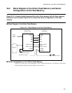
The flash memory can be accessed in 2 different ways: Flash memory mode and
alternative mode. Flash memory mode enables data to be directly written to or erased
from the external pins. Alternative mode enables data to be written to or erased from the
CPU via the internal bus. Use the mode external pins to select the mode.
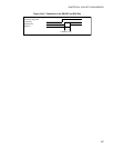
■ Flash Memory Mode
The CPU stops when the mode pins are set to "111
B
" while the reset signal is asserted. The flash memory
interface circuit is connected directly to ports 2, 4 and 5, enabling direct control from the external pins. This
mode makes the MCU seem like a standard flash memory to the external pins, and write/erase can be
performed using a flash memory programmer.
In flash memory mode, all operations supported by the flash memory automatic algorithm can be used.
■ Alternative Mode
The flash memory is located in the FF bank in the CPU memory space, and like ordinary mask ROM, can
be read-accessed and program-accessed from the CPU via the flash memory interface circuit.
Since writing/erasing the flash memory is performed by instructions from the CPU via the flash memory
interface circuit, this mode allows rewriting even when the MCU is soldered on the target board.
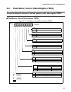
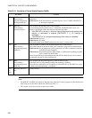
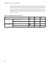
■ Flash Memory Control Signals
Table 24.3-1 lists the flash memory control signals in flash memory mode.
The flash memory control signals and the external pin of the MBM29LV200 have one-to-one relationship.
In flash memory mode, the external data bus signal width is limited to 8 bits, enabling only 1 byte access.
The DQ15 to DQ8 pins are not supported. The BYTE
pin should always be set to 0.