


34
CHAPTER 2 CPU
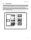
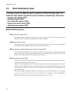
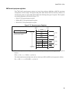
2.5 Bank Addressing Types
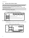
In the bank method, the 16M bytes space is divided into 256 for 64K bytes banks. The
following 5 bank registers are used to specify the banks corresponding to each space:
• Program bank register (PCB)
• Data bank register (DTB)
• User stack bank register (USB)
• System stack bank register (SSB)
• Additional bank register (ADB)
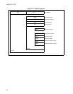
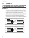
■ Bank Addressing Types
●
Program bank register (PCB)
The 64K bytes bank specified by the PCB is called a program (PC) space. The PC space contains
instruction codes, vector tables, and immediate value data, for example.
●
Data bank register (DTB)
The 64K bytes bank specified by the DTB is called a data (DT) space. The DT space contains readable/
writable data, and control/data registers for internal and external resources.
●
User stack bank register (USB)/system stack bank register (SSB)
The 64K bytes bank specified by the USB or SSB is called a stack (SP) space. The SP space is accessed
when a stack access occurs during a push/pop instruction or interrupt register saving. The S flag in the
condition code register determines the stack space to be accessed.
●
Additional bank register (ADB)
The 64K bytes bank specified by the ADB is called an additional (AD) space. The AD space, for example,
contains data that cannot fit into the DT space.
Table 2.5-1 lists the default spaces used in each addressing mode, which are pre-determined to improve
instruction coding efficiency. To use a non-default space for an addressing mode, specify a prefix code
corresponding to a bank before the instruction. This enables access to the bank space corresponding to the
specified prefix code.
After reset, the DTB, USB, SSB, and ADB are initialized to 00
H
. The PCB is initialized to a value specified
by the reset vector. After reset, the DT, SP, and AD spaces are allocated in bank 00
H
(000000
H
to
00FFFF
H
), and the PC space is allocated in the bank specified by the reset vector.