


172
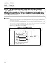
CHAPTER 10 I/O PORTS
10.2.2 Port Direction Register (DDR)
This register has following functions:
• Setting the data direction of each pin that is used as a port.
• Setting the input level of SIN -- Serial data input pin for LIN-UART.
■ Port Direction Register (DDR)
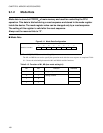
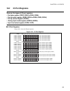
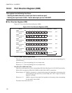
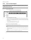
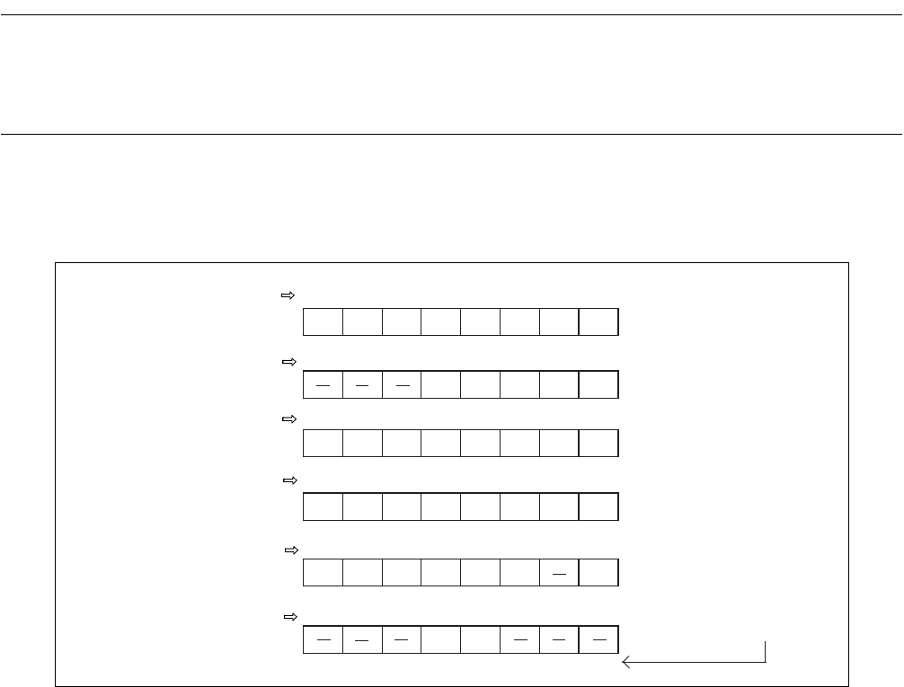
Figure 10.2-3 shows the Port Direction Registers (DDR).
Figure 10.2-3 Port Direction Registers (DDR)
Bits Dxx (DDR2, DDR4 to DDR6, DDR8)
These bits set to the I/O direction of the port. When each pin is used as port, the corresponding pin is
controlled below.
When set to "0": The corresponding pin is set to input mode.
When set to "1": The corresponding pin is set to output mode.
Bits SIL0, SIL1 (DDRA bit3, bit4)
These bits set the input level of the corresponding SIN (Serial Data Input for LIN-UART) pin forcibly.
SIL0 to SIL1 correspond to SIN0 (LIN-UART0) to SIN1(LIN-UART1), respectively.
When setting to “0”: CMOS or Automotive is selected for the input level depending on the setting of the
corresponding ILx bit and ILTx bit in the ILSR. (See "10.2.5 Input Level Select
Register" for ILSR.)
When set to “1”: CMOS is selected for the input level regardless of the setting of the corresponding
ILx bit and ILTx bit in ILSR.
The initial value of these bits is “0”.
D27 D26 D25 D24 D23 D22 D21 D20 00000000
B
R/W
D44 D43 D42 D41 D40 XXX00000
B
R/W
D54 D53 D52 D51 D50 00000000
B
R/W
D67 D66 D65 D64 D63 D62 D61 D60 00000000
B
R/W
D87 D86 D85 D84 D83 D82 D80 000000X0
B
R/W
SIL0SIL1
XXX00XXX
B
WW
D57 D56 D55
76543210
76543210
76543210
76543210
76543210
76543210
Bit No.
Reset value Access
Bit No.
Bit No.
Bit No.
Bit No.
Bit No.
DDR2
Address: 000012
H
DDR4
Address: 000014
H
DDR5
Address: 000015
H
DDR6
Address: 000016
H
DDR8
Address: 000018
H
DDRA
Address: 00001A
H
Access