9
CHAPTER 1 OVERVIEW
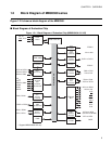
1.2 Block Diagram of MB90360 series
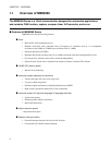
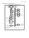
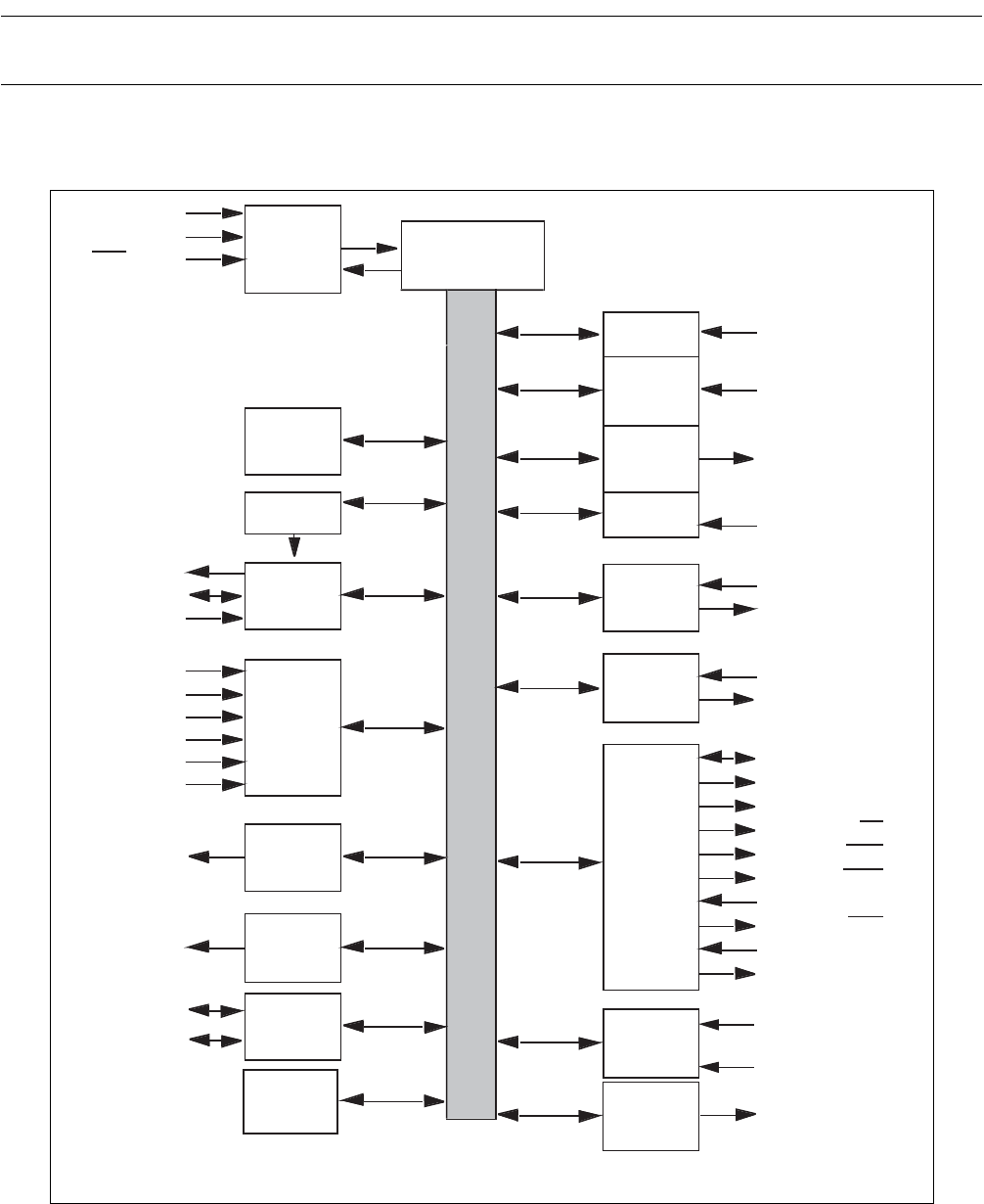
Figure 1.2-3 shows a block diagram of the MB90360.
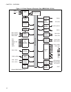
■ Block Diagram of Evaluation Chip
Figure 1.2-1 Block Diagram of Evaluation Chip (MB90V340A-101/102)
(INT15R to INT8R)
INT15 to INT8
INT7 to INT0
CKOT
SCL1, SCL0
SDA1, SDA0
PPGF to PPG0
DMA
DA01, DA00
RAM 30KB
AV
SS
AV
CC
FRCK0
IN7 to IN0
OUT7 to OUT0
FRCK1
RX2 to RX0
TX2 to TX0
TIN3 to TIN0
TOT3 to TOT0
AD15 to AD00
A23 to A16
ALE
RD
WRL
WRH
HRQ
HAK
RDY
CLK
X0, X1
X0A, X1A *
RST
SOT4 to SOT0
SCK4 to SCK0
SIN4 to SIN0
AN23 to AN0
AVRH
AVRL
ADTG
Clock
control
Prescaler
(5 channels)
8-/10-bit
A/D
converter
24 channels
10-bit
D/A
converter
2 channels
8-/16-bit
PPG
16 channels
16-bit
I/O timer 0
Input
capture
8 channels
Output
compare
8 channels
16-bit
I/O timer 1
CAN
controller
3 channels
16-bit
reload
timer
4 channels
External
bus
DTP/
external
interrupt
Clock
monitor
F
2
MC-16LX core
I
2
C
interface
2channels
*: Support MB90V340A-102 only
Internal data bus
UART
(5 channels)


