


342
CHAPTER 18 8-/10-BIT A/D CONVERTER
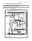
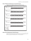
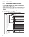
●
Details of pins in block diagram
Table 18.2-1 shows the actual pin names and interrupt request numbers of the 8-/10-bit A/D converter.
●
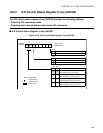
A/D control status registers (ADCS)
This register starts the A/D conversion function by software, selects the start trigger for the A/D conversion
function, selects the conversion mode, enables or disables an interrupt request, checks and clears the
interrupt request flag, temporarily stops A/D conversion and checks the state during conversion, and sets
the resolution.
●
A/D data registers (ADCR)
This register stores the A/D conversion results.
●
A/D setting register (ADSR)
Starting channel and end channel of A/D conversion, compare time of A/D conversion and sampling time
are set.
●
Start selector
This selector selects the trigger to start A/D conversion. An external pin input can be set as the start trigger.
●
Decoder
This decoder sets the A/D conversion start channel select bits and the A/D conversion end channel select
bits in the A/D control status register (ADSR0:ANS3 to ANS0 and ANE3 to ANE0) to select the analog
input pin to be used for A/D conversion.
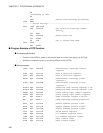
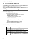
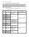
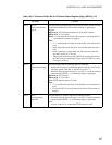
Table 18.2-1 Pins and Interrupt Request Numbers in Block Diagram
Pin Name/Interrupt Request Number in Block
Diagram
Actual Pin Name/Interrupt Request
Number
ADTG Trigger input pin P80/ADTG/INT12R
AN0 to AN7 Analog input pin ch0 to ch7
P60/AN0 to P65/AN5
P66/AN6/PPGC(D)
P67/AN7/PPGE(F)
AN8 to AN15 Analog input pin ch8 to ch15
P50/AN8 to P52/AN10
P53/AN11/TIN3
P54/AN12/TOT3/INT8
P55/AN13/INT10
P56/AN14/INT11
P57/AN15/INT13
AVR Vref+ input pin AVR
AV
CC
V
CC
input pin AV
CC
AV
SS
V
SS
input pin AV
SS
Interrupt request
output
Interrupt request output #29(1D
H
)