


402
CHAPTER 20 LIN-UART
*: Refer to the following table.
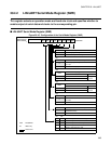
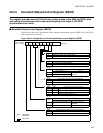
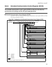
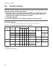
Table 20.4-4 Function in Each Bit of the Extended Status/control Register (ESCR)
NO. Bit name Function
bit15 LBIE:
LIN synch break detection
interrupt enable bit
This bit enables/disables LIN synch break detection interrupt.
When the LBD bit is set to 1 and this bit is "1", a interrupt is generated. This
bit is fixed to "0" in operation mode 1 and 2.
bit14 LBD:
LIN synch break detected
flag bit
This bit goes 1 if a LIN synch break was detected in operating mode 3.
Writing a 0 to it clears this bit and the corresponding interrupt, if it is enabled.
Read-modify-write instructions always return 1. Note that this dose not
indicate a LIN synch break detection.
Note:
When LIN synch break detection is performed, disable reception (SCR:
RXE=0) after enable LIN synch break detection interrupt (LBIE=1).
bit13,
bit12
LBL1/0:
LIN synch break length
selection bits
These two bits determine how many serial bit times the LIN synch break is
generated by LIN-UART.
Receiving a LIN synch break is always fixed to 11 bit times.
bit11 SOPE:
Serial Output pin direct
access enable bit *
Setting this bit to 1 enables the direct write to the SOTn pin, if SOE = 1
(SMR). *
bit10 SIOP:
Serial Input/Output Pin
direct access bit *
Normal read instructions always return the actual value of the SINn pin.
Writing to it sets the bit value to the SOTn pin, if SOPE = 1. During a Read-
Modify-Write instruction the bit returns the SOTn value in the read cycle. *
bit9 CCO:
Continuous Clock Output
enable bit
This bit enables a continuous serial clock output at the SCKn pin if LIN-
UART operates in master operation mode 2 (synchronous) and the SCKn pin
is configured as a clock output.
<Note> When CCO bit is "1", use SSM bit of ECCR as setting to "1".
bit8 SCES:
Sampling clock edge
selection bit
This bit inverts the serial clock signal in operation mode 2 (synchronous
communication). Receiving data is sampled at the falling edge of the internal
clock. If the MS bit of the ECCR register is "0" (master mode) and the SCKE
bit of the SMR register is "1" (clock output enabled), the output clock signal is
also inverted.
During operation mode 0,1,3, please set this bit to 0.
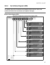
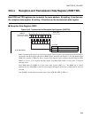
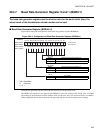
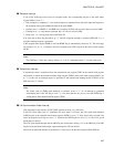
Table 20.4-5 Description of the Interaction of SOPE and SIOP
SOPE SIOP Writing to SIOP Reading from SIOP
0 R/W Has no effect on SOTn, but holds the written value Returns current value of SINn
1 R/W Write "0" or "1" to SOTn Returns current value of SINn
1 RMW Reads current value of SOTn and write it back