


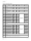

570
APPENDIX
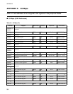
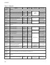
00004B
H
Reserved
00004C
H
PPGE operation mode control register
PPGCE W, R/W
16-bit
PPGE/F
0 X 0 0 0 XX1
B
00004D
H
PPGF operation mode control register PPGCF W, R/W
0 X 0 0 0 0 0 1
B
00004E
H
PPGE/F count clock selection register PPGEF R/W
0 0 0 0 0 0 X 0
B
00004F
H
Reserved
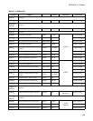
000050
H
Input capture control status 0/1 ICS01 R/W
Input Capture 0/1
0 0 0 0 0 0 0 0
B
000051
H
Input capture edge 0/1 ICE01 R/W, R
XXX0X0XX
B
000052
H
Input capture control status 2/3 ICS23 R/W
Input Capture 2/3
0 0 0 0 0 0 0 0
B
000053
H
Input capture edge 2/3 ICE23 R
XXXXXXXX
B
000054
H
to
000063
H
Reserved
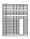
000064
H
Timer control status 2 TMCSR2 R/W
16-bit Reload Timer
2
0 0 0 0 0 0 0 0
B
000065
H
Timer control status 2 TMCSR2 R/W
XXXX 0 0 0 0
B
000066
H
Timer control status 3 TMCSR3 R/W
16-bit Reload Timer
3
0 0 0 0 0 0 0 0
B
000067
H
Timer control status 3 TMCSR3 R/W
XXXX 0 0 0 0
B
000068
H
A/D control status 0 ADCS0 R/W
A/D Converter
0 0 0 XXXX 0
B
000069
H
A/D control status 1 ADCS1 R/W, W
0 0 0 0 0 0 0 X
B
00006A
H
A/D data 0 ADCR0 R
0 0 0 0 0 0 0 0
B
00006B
H
A/D data 1 ADCR1 R
XXXXXX 0 0
B
00006C
H
ADC setting 0 ADSR0 R/W
0 0 0 0 0 0 0 0
B
00006D
H
ADC setting 1 ADSR1 R/W
0 0 0 0 0 0 0 0
B
00006E
H
Detection reset control register of
low-voltage/CPU operation
LVRC R/W, W
Detection Reset of
Low-voltage/CPU
Operation
0 0 1 1 1 0 0 0
B
00006F
H
ROM mirror function select ROMM W ROM Mirror
XXXXXXX1
B
000070
H
to
00007F
H
Reserved
000080
H
to
00008F
H
Reserved for CAN interface. (For more information, see Table 21.3-1 .)
000090
H
to
00009D
H
Reserved
00009E
H
Address detection control register0 PACSR0 R/W
Address Match
Detection 0
0 0 0 0 0 0 0 0
B
Table A-1 I/O Map (3/5)
Address Register
Abbreviation
Access Peripheral Initial value