102
CHAPTER 5 CLOCKS
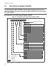
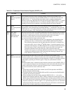
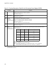
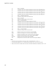
Table 5.4-1 Functional Description of Each Bit in the PLL/subclock Control Register (PSCCR)
Bit name Function
bit15
to
bit12
Unused These bits are not used.
Writing to these bits has no effect to operation.
Read value is always "1".
bit11 Reserved bit Always write "0" to this bit.
Read value is always "1".
bit10 SCDS:
Subclock
division selection
bit
The division ratio of the subclock is selected.
When "0" is written to this bit, 4 division is selected.
When "1" is written to this bit, 2 division is selected.
Read value is always "1".
This bit is initialized to "0" by all reset causes.
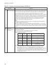
bit9 Reserved bit Always write "0" to this bit.
Read value is always "1".
bit8 CS2:
Multiplication
rate selection bit
This bit and CS1 and CS0 bits of the clock selection register (CKSCR) determine the PLL
multiplication rate.
CS2 CS1 CS0 PLL clock multiplication rate
000 × 1
001 × 2
010 × 3
011 × 4
110 × 6
1 1 1 Setting disabled
Read value is always "1".
This bit is initialized to "0" by all reset causes.
Note: When MCS or MCM bit is "0", setting CS2 to CS0 to "111
B
" is prohibited.
When CKSCR: CS1 and CS0 is set to "11
B
", do not set "1" to this bit.
Note: PSCCR register is write-only register. Read value is different from writing value. Do not use the RMW instruction
(SETB/CLRB instruction).


