543
CHAPTER 24 512K-BIT FLASH MEMORY
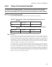
24.6.3 Timing Limit Exceeded Flag (DQ5)
The timing limit exceeded flag (DQ5) is used to post that execution of the automatic
algorithm has exceeded the time (internal pulse count) prescribed in the flash memory.
■ Timing Limit Exceeded Flag (DQ5)
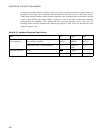
Table 24.6-7 and Table 24.6-8 list the state transitions of the timing limit exceeded flag.
●
Write/chip erase
Read-access after write or chip erase automatic algorithm activation causes the flash memory to output 0 if
the time is within the prescribed time (time required for write/erase) or to output 1 if the prescribed time
has been exceeded. Because this is done regardless of whether the automatic algorithm is being executed or
has terminated, it is possible to determine whether write/erase was successful or unsuccessful. That is,
when this flag outputs 1, writing can be determined to have been unsuccessful if the automatic algorithm is
still being executed by the data polling function or toggle bit function.
For example, writing 1 to a flash memory address where 0 has been written will cause the fail state to
occur. In this case, the flash memory will lock and execution of the automatic algorithm will not terminate.
In rare cases normal termination may be seen as with the case where "1" can be written. As a result, valid
data will not be outputted from the data polling flag (DQ7). In addition, the toggle bit flag (DQ6) will
exceed the time limit without stopping the toggle operation and the timing limit exceeded flag (DQ5) will
output 1. Note that this state indicates that the flash memory is not faulty, but has not been used correctly.
When this state occurs, execute the Reset command.
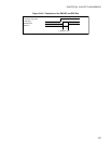
Table 24.6-7 State Transition of Timing Limit Exceeded Flag (State change at normal
operation)
Operating State Programming
→ Completed
Chip Erasing → Completed
DQ5 0 → DATA:5 0 → 1
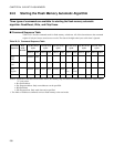
Table 24.6-8 State Transition of Timing Limit Exceeded Flag (State change at abnormal
operation)
Operating State Programming Chip Erasing
DQ5 1 1


