


5-31
DEVICE CONFIGURATION
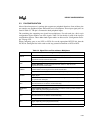
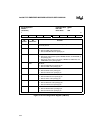
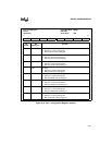
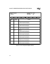
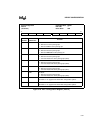
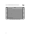
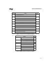
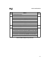
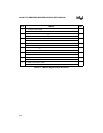
Table 5-5. Example DMACFG Configuration Register
Bit # DMACFG Value
7 0 = Enables DACK1# at chip pin 1
1 = Disables DACK1# at chip pin
6–4 000 = DRQ1 pin (external peripheral) connected to DREQ1 000
001 = SIO channel 1’s receive buffer full signal (RBFDMA1) connected to DREQ1
010 = SIO channel 0’s transmit buffer empty signal (TXEDMA0) to DREQ1
011 =SSIO receive holding buffer full signal (SSRBF) to DREQ1
100 = TCU counter 2’s output signal (OUT2) to DREQ1
101 = SIO channel 0’s receive buffer full signal (RBFDMA0) to DREQ1
110 = SIO channel 1’s transmit buffer empty signal (TXEDMA1) to DREQ1
111 = SSIO transmit holding buffer empty signal (SSTBE) to DREQ1
3 0 = Enables DACK0# at chip pin 1
1 = Disables DACK0# at chip pin
2–0 000 = DRQ0 pin (external peripheral) connected to DREQ0 000
001 = SIO channel 0’s receive buffer full signal (RBFDMA0) connected to DREQ0
010 = SIO channel 1’s transmit buffer empty signal (TXEDMA1) connected to DREQ0
011 = SSIO transmit holding buffer empty signal (THBE) connected to DREQ0
100 = TCU counter 1’s output signal (OUT1) connected to DREQ0
101 = SIO channel 1’s receive buffer full signal (RBFDMA1) connected to DREQ0
110 = SIO channel 0’s transmit buffer empty signal (TXEDMA0) connected to DREQ0
111 = SSIO receive holding buffer full signal (RHBF) connected to DREQ0