


Intel386™ EX EMBEDDED MICROPROCESSOR USER’S MANUAL
6-28
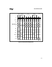
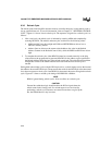
6.3.6 Refresh Cycle
The refresh control unit simplifies dynamic memory controller design by issuing dummy read cy-
cles at specified intervals. (For more information, refer to Chapter 15, “REFRESH CONTROL
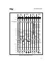
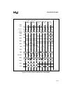
UNIT.”) Figure 6-11 shows a basic refresh cycle. The sequence of signals for a refresh cycle is as
follows:
1. Like a read cycle, the refresh cycle is initiated by asserting ADS# and completed by
asserting READY#. The address and status pins are driven to the following values:
• M/IO# and D/C# are driven high and W/R# and REFRESH# are driven low to
indicate a memory refresh.
• Address lines are driven to the current refresh address (the value in the Refresh
Address Counter in the Refresh Control Unit), while the BHE# and BLE# are driven
high.
2. To complete the refresh cycle, either READY# must be asserted externally or the chip
select unit must be programmed to generate READY# for the address region specified in
the Refresh Address Base Register in the refresh control unit. The refresh control unit then
relinquishes control to the current internal bus master until the next refresh cycle is
needed.
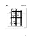
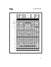
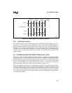
During hold acknowledge cycles with the HLDA pin active, a refresh request causes the internal
bus arbiter to deassert the HLDA pin. The processor then waits for the HOLD pin to be deasserted
for at least one processor clock cycle. Once HOLD is deasserted, the processor begins the refresh
cycle. Figure 6-12 shows a refresh cycle during a HOLD/HLDA condition.
NOTE
BS8# is ignored during refresh cycles. It has no effect on a refresh cycle.
CAUTION
External bus arbitration logic should monitor the HLDA signal when the
refresh control unit is being used. If a refresh request is not serviced (by
performing a refresh cycle) because an external master does not give up the
bus, the DRAM devices may lose data.