6-31
BUS INTERFACE UNIT
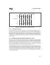
6.3.7 BS8 Cycle
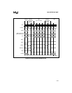
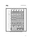
The BS8 cycle allows external logic to dynamically switch between an 8-bit data bus size and a
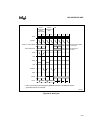
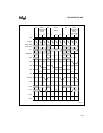
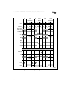
16-bit data bus size, by using the BS8# signal. Figure 6-13 shows a word access to an 8-bit pe-
ripheral.
To use the dynamic 8-bit bus sizing, an external memory or I/O should connect to the lower eight
bits of the data bus (D7:0), use the BLE# as address bit 0, and assert BS8# (at the BS8# pin) in
T2 of a memory or I/O access. A BS8 cycle can also be generated by the internal chip-select unit
(Refer to Chapter 14, “CHIP-SELECT UNIT”). In this case, the Chip Select Unit generates the
BS8# signal internally.
Depending upon the current bus access width and address and the state of the BS8# signal, the
processor performs the actions described in the next two sections.
6.3.7.1 Write Cycles
• If the current bus cycle is a byte write with BHE# active and BLE# inactive, the processor
copies the upper eight bits of the data bus (D15:8) to the lower eight bits of the data bus
(D7:0), i.e. the byte appears on both the upper and lower data buses.
• If the current bus cycle is a byte write with BHE# inactive and BLE# active, the processor
ignores the state of the BS8# signal.
• If the current bus cycle is a word write with both BHE# and BLE# active and the processor
samples the BS8# signal active at the end of the last T2 (when READY# is sampled active),
the processor waits for the current bus to complete and then executes another write cycle
with the upper eight bits of the data bus (D15:8) copied to the lower eight bits of the data
bus (D7:0). The processor deactivates BLE# on the second cycle (BLE# is used as address
A0 to an 8-bit device; this translates to A0=0 for the first cycle and A0=1 for the second).
6.3.7.2 Read Cycles
• If the current bus cycle is a byte read with BHE# active and BLE# inactive, and the
processor samples the BS8# signal active at the end of the last T2 (when READY# is
sampled active), the processor latches the data on the lower eight bits of the data bus (D7:0)
and internally routes this data to the upper data bus of the core.
• If the current bus cycle is a byte read with BHE# inactive and BLE# active, the processor
ignores the state of the BS8# signal.
• If the current bus cycle is a word read with both BHE# and BLE# active and the processor
samples the BS8# signal active at the end of the last T2 (when READY# is sampled active),
the processor waits for the current bus cycle to complete and latches the data on the lower
eight bits of the data bus (D7:0). It then executes another read cycle, with BLE# inactive
(BLE# is used as address A0 to an 8-bit device; this translates to A0=0 for the first cycle
and A0=1 for the second), latching the data on the lower eight bits of the data bus (D7:0)
again and using it.


