


Intel386™ EX EMBEDDED MICROPROCESSOR USER’S MANUAL
11-32
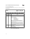
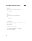
11.3.12 Scratch Pad Register (SCR
n
)
SCRn is available for use as a scratch pad. Writing and reading this register has no effect on SIOn
operation.
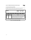
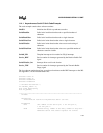
Figure 11-23. Scratch Pad Register (SCR
n
)
11.4 PROGRAMMING CONSIDERATIONS
Consider the following when programming the SIO.
• The divisor latch low register (DLLn) is multiplexed with the receive and transmit buffer
registers (RBRn and TBRn) and the divisor latch high register (DLHn) is multiplexed with
the interrupt enable register (IERn). Bit 7 of the serial line control register (LCRn) controls
which register is accessed.
• The SIO contains four status signals: receiver line status, receive buffer full, transmit buffer
empty, and modem status. You can connect (OR) these signals to the interrupt control unit’s
SIOINTn interrupt request signal using the interrupt enable register (IERn). If you receive
an interrupt request on the SIOINTn signal, read the interrupt ID register (IIRn) to
determine which status signal with the highest priority caused the request.
Several sources can activate the receiver line status and the modem status signals. If IIRn
indicates that the receiver line status signal caused an interrupt request, read the serial line
status register (LSRn) to determine the receive error condition that activated the receiver
line status signal. If IIRn indicates that the modem status signal caused an interrupt request,
read the modem status register (MSRn) to determine which modem input signal activated
the modem status signal.
• DMA can be used for servicing the SIO channels for higher baud rates. When doing this,
remember that the isolated RBF and TBE (RBFDMA and TBEDMA) signals are connected
to the DMA DREQ inputs. RBFDMA is blocked if any of the error bits in the LSR are set.
Neither signal is gated by the IERn register.
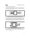
Scratch Pad
SCR0, SCR1
(read/write)
Expanded Addr:
ISA Addr:
Reset State:
SCR0 SCR1
F4FFH F8FFH
03FFH 02FFH
XXH XXH
7 0
SP7 SP6 SP5 SP4 SP3 SP2 SP1 SP0
Bit
Number
Bit
Mnemonic
Function
7–0 SP7:0 Writing and reading this register has no effect on SIO
n
operation.