Intel386™ EX EMBEDDED MICROPROCESSOR USER’S MANUAL
18-12
18.4 TIMING INFORMATION
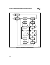
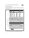
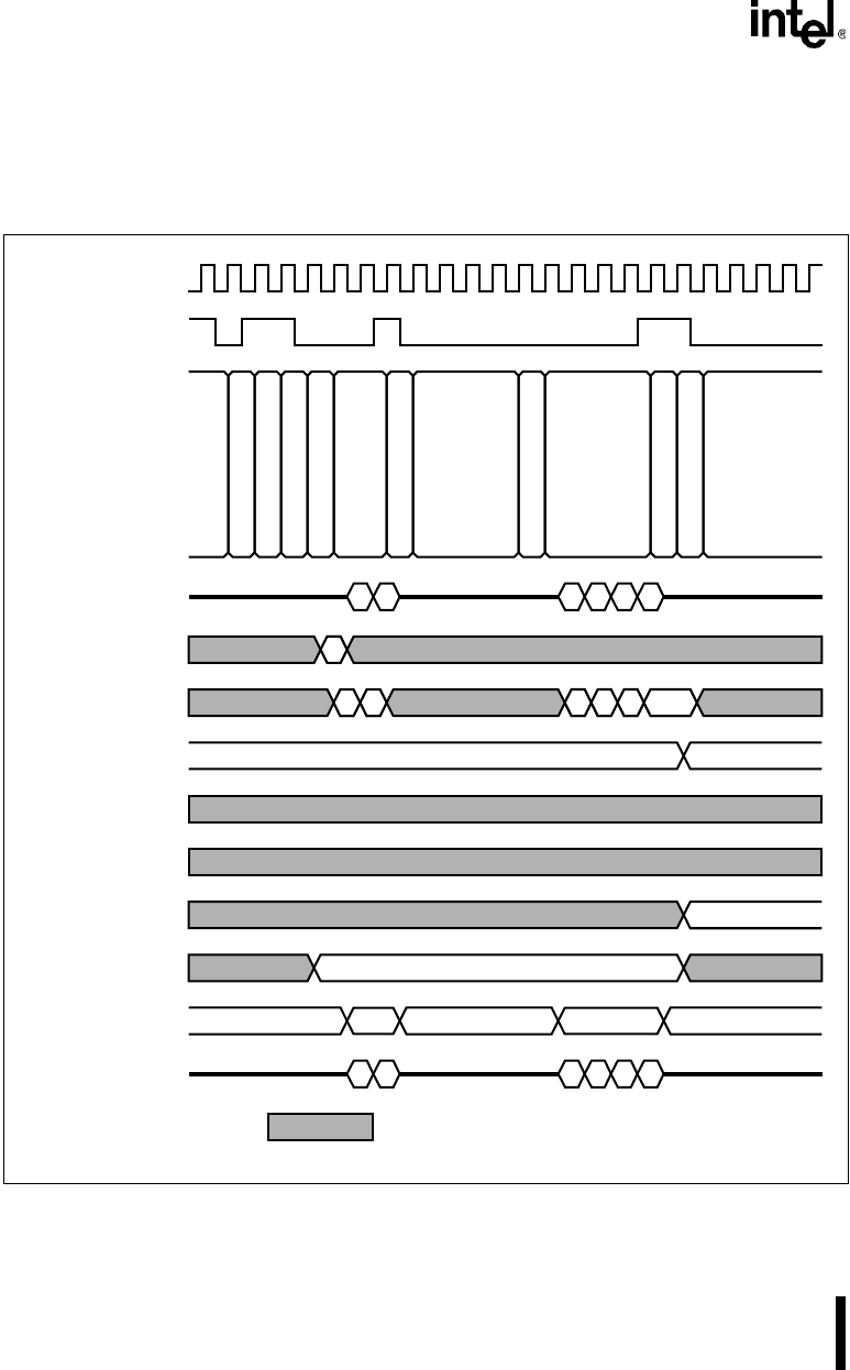
The test-logic unit’s input/output timing is as specified in IEEE 1149.1. Figure 18-5 shows the
pin timing associated with loading the instruction register and Figure 18-6 shows the timing for
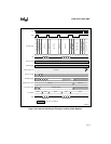
loading a given data register.
Figure 18-5. Internal and External Timing for Loading the Instruction Register
A2361-01
Test - Logic - Reset
Run - Test / Idle
Select - DR - Scan
Select - IR - Scan
Capture - IR
Shift - IR
Exit1 - IR
Pause - IR
Exit2 - IR
Shift - IR
Exit1 - IR
Update - IR
Run - Test / Idle
TDI
Data Input to IR
IR Shift-Register
Parallel Output of IR
Data Input to TDR
TDR Shift-Register
Parallel Output of TDR
Register Selected
TDO Enable
TDO
= Don't care or undefined.
IDCode
New Instruction
Old Data
Instruction Register
Inactive
Active Inactive
Active
Inactive
Controller State
TMS
TCK


