15-11
REFRESH CONTROL UNIT
15.5 DESIGN CONSIDERATIONS
Consider the following when programming the RCU.
• The system address bus does not contain an address A0 signal; instead, it uses the BLE#
and the BHE# pins to generate the lowest address bit. During all refresh operations, BLE#
and BHE# are driven high.
This needs to be noted especially when interfacing to an 8-bit wide Pseudo Static RAM
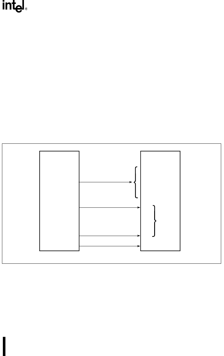
(PSRAM) device. The lowest address bit generated by the refresh address counter is A1. A
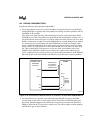
circuit like the one shown in Figure 15-6 can be used to ensure the refresh of all rows. Here
BLE# is connected to an address line of the PSRAM that is not used during refresh. Address
A1 of the processor is connected to A0 of the PSRAM and so forth. For example, when
using a 128Kx8-bit PSRAM device (refresh cycles only use the address present on inputs
A8:0), connect A1 of the processor to A0 of the PSRAM, A2 to A1 and so on, until A9 to
A8. Then connect BLE# of the processor to any one of the A16:9 address lines of the
PSRAM. Since PSRAM is random access memory, this scheme works. During access
cycles, sequential accesses by the processor go to non-contiguous addresses in the PSRAM,
but since the processor does both the read and write cycles, this does not pose a problem.
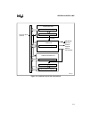
Figure 15-6. Connections to Ensure Refresh of All Rows in an 8-Bit Wide PSRAM Device
• An external device can gain bus control through either the HOLD signal or the DMA
cascade mode. In this case, a refresh request causes the HLDA or DACKn# signal to be
deasserted. When this happens, the external device must drop its request line (HOLD or
DRQn) to allow the RCU to perform a refresh cycle. The refresh request remains pending
until the RCU gets control of the bus.
Intel386™ EX
Embedded
Processor
A
m
.
.
.
A1
A0
PSRAM
BLE# can be
connected to
any of these
address lines
A
m+1
.
.
.
A2
A1
BLE#
A3352-02
A
n
.
.
.
.
A
m+1
Used
during
refresh
cycles


