15-9
REFRESH CONTROL UNIT
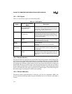
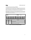
15.4.3 Refresh Base Address Register (RFSBAD)
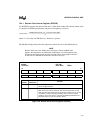
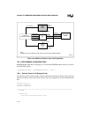
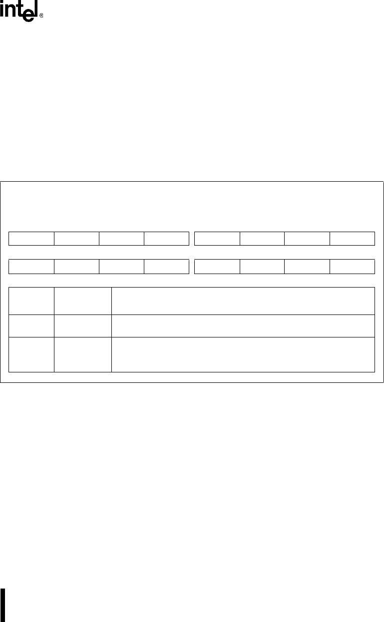
Use RFSBAD to set up the memory region that needs refreshing. The value written to this register
forms the upper bits (A25:14) of the refresh address. The RFSBAD register can be used in con-
junction with the Chip Select Unit (CSU) to generate a chip-select for the DRAM region during
refresh cycles. If the address in the RFSBAD matches the region programmed in the CSU for
DRAM, then the DRAM chip-select is generated for both access and refresh cycles.
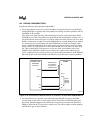
By programming two separate regions in the CSU, one for DRAM access cycles and the other for
DRAM refresh cycles, separate chip-selects can be generated for the two types of cycles. In this
case, the RFSBAD needs to be programmed with an address that matches the CSU region that is
programmed for the refresh cycle chip-select.
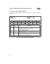
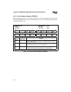
Figure 15-4. Refresh Base Address Register (RFSBAD)
Refresh Base Address
RFSBAD
(read/write)
Expanded Addr:
ISA Addr:
Reset State:
F4A0H
—
0000H
15 8
— — — — RA25 RA24 RA23 RA22
7 0
RA21 RA20 RA19 RA18 RA17 RA16 RA15 RA14
Bit
Number
Bit
Mnemonic
Function
15–12 — Reserved. These bits are undefined; for compatibility with future devices,
do not modify these bits.
11–0 RA25:14 Refresh Base:
These bits make up the A25:14 address bits of the refresh address. This
establishes a memory region for refreshing.


