


6-13
BUS INTERFACE UNIT
6.3 BUS CYCLES
The processor executes five types of bus cycles:
• Read
• Write
• Interrupt
• Halt/shutdown
• Refresh
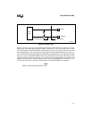
6.3.1 Read Cycle
Read cycles are of two types:
• In a pipelined cycle, the address and status signals are output in the previous bus cycle, to
allow longer memory access times. Pipelined cycles are described in “Pipelined Cycle” on
page 6-19.
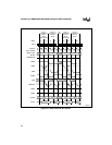
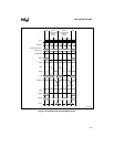
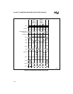
• In a nonpipelined cycle, the address and status signals become valid during the first T-state
of the cycle (T1). Figure 6-5 shows the timing for two nonpipelined read cycles (one with
and one without a wait-state).
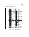
The sequence of signals for the nonpipelined read cycle is as follows:
1. The processor initiates the cycle by driving the address bus and the status signals active
and asserting ADS#. The type of bus cycle occurring is determined by the states of the
address bus (A25:1), byte enable pins (BLE# and BHE#), and bus status outputs (W/R#,
M/IO#, D/C#, REFRESH#, and LOCK#). Because of output delays, these signals should
be sampled at the rising edge of the CLK2 signal that coincides with the falling edge of
PH2, when ADS# is definitely active. For a read cycle, the bus status outputs have the
following states:
• W/R# is low
• M/IO# is high for a memory read and low for an I/O read
• D/C# is high for a memory or I/O data read and low for a memory code read
• REFRESH# is deasserted
• LOCK# is asserted for a locked cycle and deasserted for a nonlocked cycle. In a read-
modify-write sequence, both the memory data read and memory data write cycles are
locked. No other bus master should be permitted to control the bus between two
locked bus cycles.
The address bus, byte enable pins, and bus status pins (with the exception of ADS#)
remain active through the end of the read cycle.
2. At the start of phase 2 of T1, RD# becomes active as the processor prepares the data bus
for input. This indicates that the processor is ready to accept data.