


Intel386™ EX EMBEDDED MICROPROCESSOR USER’S MANUAL
A-2
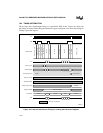
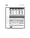
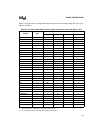
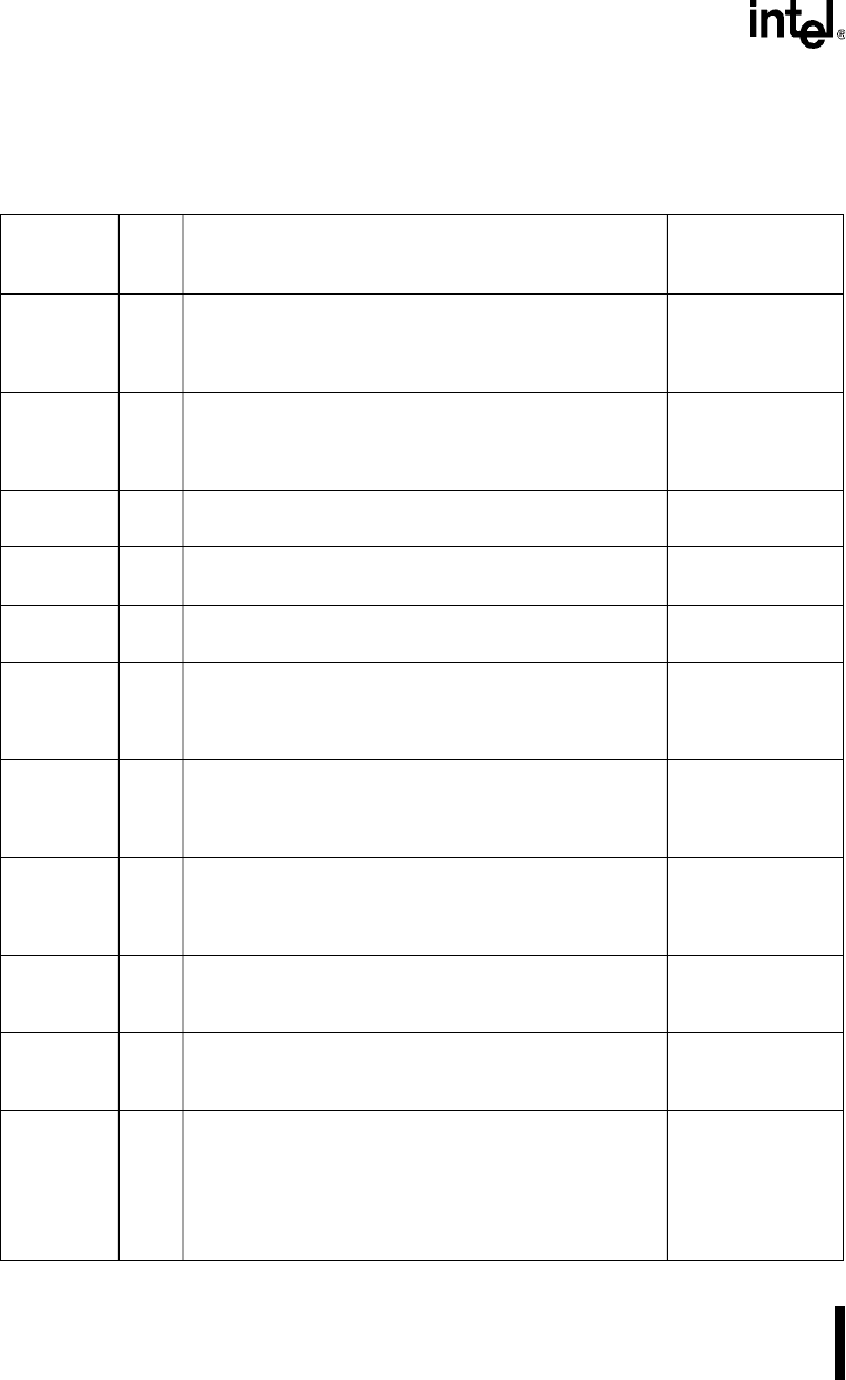
Table A-2 is an alphabetical list of the signals available at the device pins. The Multiplexed With
column lists other signals that share a pin with the signal listed in the Signal column.
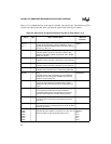
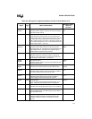
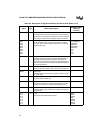
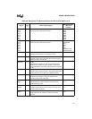
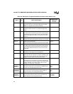
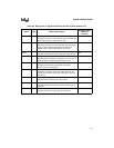
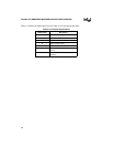
Table A-2. Description of Signals Available at the Device Pins (Sheet 1 of 6)
Signal Type Name and Description
Multiplexed With
(Alternate
Function)
A25:19
A18:16
A15:1
O Address Bus:
Outputs physical memory or port I/O addresses. These
signals are valid when ADS# is active and remain valid until
the next T1, T2P, or Ti.
—
CAS2:0
—
ADS# O Address Status:
Indicates that the processor is driving a valid bus-cycle
definition and address (W/R#, D/C#, M/IO#, A25:1, BHE#,
BLE#) onto its pins.
—
BHE# O Byte High Enable:
Indicates that the processor is transferring a high data byte.
—
BLE# O Byte Low Enable:
Indicates that the processor is transferring a low data byte.
—
BS8# I Bus Size:
Indicates that an 8-bit device is currently being addressed.
—
BUSY# I Busy:
Indicates that the math coprocessor is busy. If BUSY# is
sampled low at the falling edge of RESET, the processor
performs an internal self test.
TMRGATE2
CAS2:0 O Cascade Address:
Carries the slave address information from the master
8259A interrupt module during interrupt acknowledge bus
cycles.
A18:16
CLK2 ST Input Clock:
Is connected to an external clock that provides the
fundamental timing for the microprocessor. The internal
processor clock frequency is half the CLK2 frequency.
—
CLKOUT O Clock Output:
Use this output to synchronize external devices with the
processor.
—
COMCLK I SIO Baud Clock:
An external source connected to this pin can clock the SIO
n
baud-rate generator.
P3.7
CS6#
CS5#
CS4#
CS3#
CS2#
CS1#
CS0#
O Chip-selects:
Activated when the address of a memory or I/O bus cycle is
within the address region programmed by the user.
REFRESH#
DACK0#
P2.4
P2.3
P2.2
P2.1
P2.0