Intel386™ EX EMBEDDED MICROPROCESSOR USER’S MANUAL
A-6
SMI# ST System Management Interrupt:
Causes the device to enter System Management Mode.
SMI# is the highest priority external interrupt.
—
SMIACT# O System Management Interrupt Active:
Indicates that the processor is in System Management
Mode.
—
SRXCLK I/O SSIO Receive Clock:
In master mode, the baud-rate generator’s output appears
on SRXCLK and can be used to clock a slave transmitter. In
slave mode, SRXCLK functions as an input clock for the
receiver.
DTR1#
SSIORX I SSIO Receive Serial Data:
Accepts serial data (most-significant bit first) into the SSIO.
RI1#
SSIOTX O SSIO Transmit Serial Data:
Sends serial data (most-significant bit first) from the SSIO.
RTS1#
STXCLK I/O SSIO Transmit Clock:
In master mode, the baud-rate generator’s output appears
on STXCLK and can be used to clock a slave receiver. In
slave mode, STXCLK functions as an input clock for the
transmitter.
DSR1
TCK I Test Clock Input:
Provides the clock input for the test-logic unit.
—
TDI I Test Data Input:
Serial input for test instructions and data. Sampled on the
rising edge of TCK; valid only when either the instruction
register or a data register is being serially loaded.
—
TDO O Test Data Output:
Serial output for test instructions and data. TDO shifts out
the contents of the instruction register or the selected data
register (LSB first) on the falling edge of TCK. If serial
shifting is not taking place, TDO floats.
—
TMRCLK2
TMRCLK1
TMRCLK0
I Timer/Counter Clock Input:
An external clock source connected to the TMRCLK
n
pin
can drive the corresponding timer/counter.
PEREQ
INT6
INT4
TMRGATE2
TMRGATE1
TMRGATE0
I Timer/Counter Gate Input:
Can control the counter’s operation (enable, disable, or
trigger, depending on the programmed mode).
BUSY#
INT7
INT5
TMROUT2
TMROUT1
TMROUT0
O Timer/Counter Output:
Can provide the timer/counter’s output. The form of the
output depends on the programmed mode.
ERROR#
P3.1/INT8
P3.0/INT9
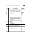
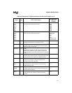
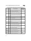
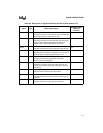
Table A-2. Description of Signals Available at the Device Pins (Sheet 5 of 6)
Signal Type Name and Description
Multiplexed With
(Alternate
Function)


