6-1
CHAPTER 6
BUS INTERFACE UNIT
The processor communicates with memory, I/O, and other devices through bus operations. Ad-
dress, data, status, and control information define a bus cycle. The Bus Interface Unit supports
read and write cycles to external memory and I/O devices. It also contains the signals that allow
external bus masters to request and acquire control of the bus. The Bus Interface Unit (BIU) can
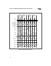
execute memory read/write cycles, I/O read/write cycles, interrupt acknowledge cycles, refresh
cycles and processor halt/shutdown cycles.
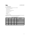
This chapter is organized as follows:
• Overview (see below)
• Bus Operation (page 6-5)
• Bus Cycles (page 6-13)
• Bus Lock (page 6-34)
• External Bus Master Support (Using HOLD, HLDA) (page 6-35)
• Design Considerations (page 6-38)
6.1 OVERVIEW
The Intel386™ EX processor’s external bus is controlled by the bus interface unit (BIU). To com-
municate with memory and I/O, the external bus consists of a data bus, a separate address bus,
seven bus status pins, two data status pins, and three control pins.
• Bidirectional data bus (D15:0) can transfer 8 or 16 bits of data per cycle.
• Address bus includes the address pins (A25:1), a high-byte-enable pin (BHE#), and a low-
byte-enable pin (BLE#). Address pins select a word in memory, and byte-enable pins select
the byte within the word to access.
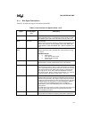
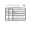
• Bus status pins include:
— ADS# indicates the start of a bus cycle and valid address bus outputs.
— W/R# identifies the bus cycle as a write or a read.
— M/IO# identifies the bus cycle as a memory or I/O access.
— D/C# identifies the bus cycle as a data or control cycle.
— LOCK# identifies a locked bus cycle.
— LBA# indicates that the processor generates an internal READY# for the current bus
cycle.
— REFRESH# identifies a refresh bus cycle.


