5-19
DEVICE CONFIGURATION
5.2.6 Chip-select Unit and Clock and Power Management Unit Configuration
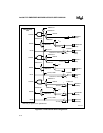
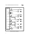
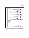
Figure 5-12 shows the multiplexing of signals of the Chip-select Unit and the Clock and Power
Management Unit.
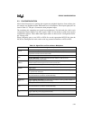
The Chip-select signals, CS6# and CS5# are multiplexed with the REFRESH# signal from the
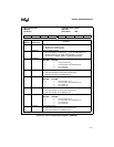
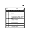
Refresh Control Unit and the DACK0# signal from the DMA Unit, respectively. Bits 6 and 4 in
the PINCFG register (see Figure 5-15) control these multiplexers. CS3#, CS2#, CS1# and CS0#
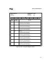
are multiplexed with I/O Port 2 signals, P2.3, P2.2, P2.1 and P2.0, respectively. Bits 4:0 in the
P2CFG register (see Figure 5-17) control these multiplexers.
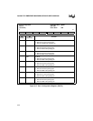
The PWRDOWN output signal of the Clock and Power Management Unit is multiplexed with
I/O Port 3 signal, P3.6. Bit 6 in the P3CFG register (see Figure 5-18) controls this multiplexer.


