


15-1
CHAPTER 15
REFRESH CONTROL UNIT
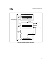
The Refresh Control Unit (RCU) simplifies the interface between the processor and a dynamic
random access memory (DRAM) device by providing a way to generate periodic refresh requests
and refresh addresses. These refresh requests and addresses can then be used by an external
DRAM controller to generate the appropriate DRAM signals and addresses needed to perform
refresh operations. The RCU can be used in conjunction with the Chip-select Unit to generate
chip select signals for DRAM regions; these signals can be used by the external DRAM controller
to initiate refresh cycles.
The RCU can also be used when interfacing to pseudo-static random access memory (PSRAM).
This type of memory has an interface similar to a static random access memory (SRAM), but re-
quires a periodic refresh similar to DRAM.
This chapter is organized as follows:
• Dynamic Memory Control (see below)
• Refresh Control Unit Overview (page 15-2)
• RCU Operation (page 15-5)
• Register Definitions (page 15-6)
• Design Considerations (page 15-11)
• Programming Considerations (page 15-14)
15.1 DYNAMIC MEMORY CONTROL
Typical DRAM devices require control logic to enable read, write, and refresh operations. The
RCU simplifies control logic design requirements by providing the necessary cell access require-
ments for refresh operations.
DRAM devices are built as matrices of memory cells. Therefore, each memory cell has a row and
column address associated with it. A typical controller design strobes addresses into a DRAM de-
vice through the use of two control lines: a row address strobe (RAS#) and a column address
strobe (CAS#). The controller presents lower (or row) address bits during RAS# and upper (or
column) address bits during CAS#. Activating RAS# accesses all cells within the specified row.
Accessing a cell refreshes it; therefore, cycling through the row addresses refreshes a DRAM de-
vice.
15.1.1 Refresh Methods
There are two common methods for refreshing a DRAM device: RAS#-only and CAS#-before-
RAS#. The DRAM controller design requirements are simpler for RAS#-only than for CAS#-be-
fore-RAS#.