8-1
CHAPTER 8
CLOCK AND POWER MANAGEMENT UNIT
The clock generation circuitry provides uniform, nonoverlapping clock signals to the core and in-
tegrated peripherals. The power management features control the clock signals to provide power
conservation options.
This chapter is organized as follows:
• Overview (see below)
• Controlling the PSCLK Frequency (page 8-7)
• Controlling Power Management Modes (page 8-8)
• Design Considerations (page 8-11)
• Programming Considerations (page 8-13)
8.1 OVERVIEW
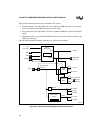
The clock and power management unit (Figure 8-1) includes clock generation, power manage-
ment, and system reset circuitry. It also provides a clock output signal (CLKOUT) for synchro-
nizing external logic to the processor’s system clock. CLKOUT is the PH1P clock.
8.1.1 Clock Generation Logic
An external oscillator must provide an input signal to CLK2, which provides the fundamental
timing for the processor. As Figure 8-1 shows, the clock generation circuitry includes two divide-
by-two counters and a programmable clock divider. The first divide-by-two counter divides the
CLK2 frequency to generate two clocks (PH1 and PH2). For power management, independent
clock signals are routed to the core (PH1C and PH2C) and to the internal peripherals (PH1P and
PH2P).
The second divide-by-two counter divides the processor clock to generate a clock input (SER-
CLK) for the baud-rate generators of the asynchronous and synchronous serial I/O units. The
SERCLK frequency is half the internal clock frequency, or CLK2/4.
The programmable divider generates a prescaled clock (PSCLK) input for the timer/counter and
synchronous serial I/O units. The maximum PSCLK frequency is the internal clock frequency di-
vided by 2 (CLK2/4) and the minimum is the internal clock frequency divided by 513
(CLK2/1026).


